IRL3714ZPbF Description
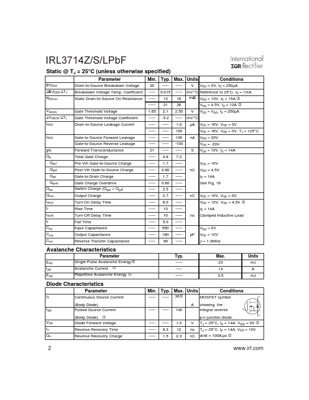
4.3 62 40 Units V A W W/°C °C Units °C/W 1 7/30/04 IRL3714Z/S/LPbF Static @ TJ = 25°C (unless otherwise specified) Parameter Min. Units Conditions BVDSS ∆ΒVDSS/∆TJ RDS(on) VGS(th) ∆VGS(th)/∆TJ Drain-to-Source Breakdown Voltage Breakdown Voltage Temp. 23 14 3.5 Units mJ A mJ Diode Characteristics Parameter IS Continuous Source Current gMin.
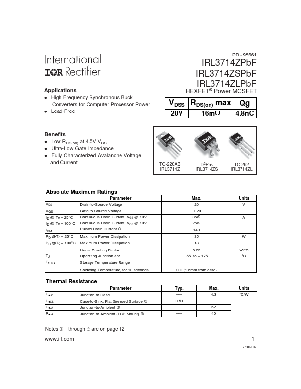
IRL3714ZPbF Key Features
- High Frequency Synchronous Buck Converters for puter Processor Power
- Lead-Free PD - 95661 IRL3714ZPbF IRL3714ZSPbF IRL3714ZLPbF HEXFET® Power MOSFET VDSS RDS(on) max Qg :20V
- Low RDS(on) at 4.5V VGS
- Ultra-Low Gate Impedance