IRL5602SPBF
IRL5602SPBF is POWER MOSFET manufactured by International Rectifier.
Description
Fifth Generation HEXFETs from International Rectifier utilize advanced processing techniques to achieve extremely low on-resistance per silicon area. This benefit, bined with the fast switching speed and ruggedized device design that HEXFET Power MOSFETs are well known for, provides the designer with an extremely efficient and reliable device for use in a wide variety of applications. The D2Pak is a surface mount power package capable of acmodating die sizes up to HEX-4. It provides the highest power capability and the lowest possible on-resistance in any existing surface mount package. The D2Pak is suitable for high current applications because of its low internal connection resistance and can dissipate up to 2.0W in a typical surface mount application.
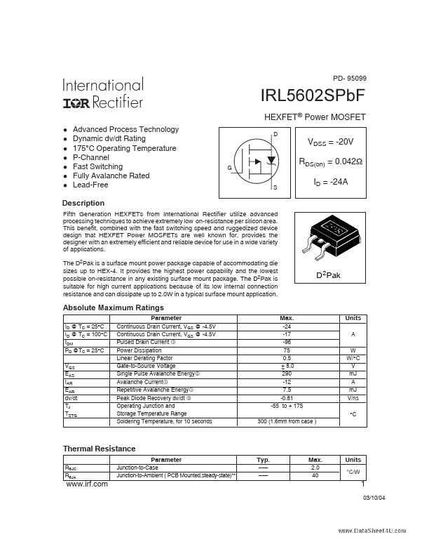
D 2 Pak
Absolute Maximum Ratings
Parameter
ID @ TC = 25°C ID @ TC = 100°C IDM PD @TC = 25°C VGS EAS IAR EAR dv/dt TJ TSTG Continuous Drain Current, VGS @ -4.5V Continuous Drain Current, VGS @ -4.5V Pulsed Drain Current Power Dissipation Linear Derating Factor Gate-to-Source Voltage Single Pulse Avalanche Energy Avalanche Current Repetitive Avalanche Energy Peak Diode Recovery dv/dt
- Operating Junction and Storage Temperature Range Soldering Temperature, for 10 seconds
Max.
-24 -17 -96 75 0.5 ± 8.0 290 -12 7.5 -0.81 -55 to + 175 300 (1.6mm from case )
Units
A W W/°C V m J A m J V/ns °C
Thermal Resistance
Parameter
RθJC RθJA Junction-to-Case Junction-to-Ambient ( PCB Mounted,steady-state)-
- Typ.
- -
- -
- -
Max.
2.0 40
Units
°C/W
.irf.
03/10/04
IRL5602SPb F
Electrical Characteristics @ TJ = 25°C (unless otherwise specified)
V(BR)DSS
∆V(BR)DSS/∆TJ
Parameter Drain-to-Source Breakdown Voltage Breakdown Voltage Temp. Coefficient Static Drain-to-Source On-Resistance Gate Threshold Voltage Forward Transconductance Drain-to-Source Leakage Current Gate-to-Source Forward Leakage Gate-to-Source Reverse Leakage Total Gate Charge Gate-to-Source Charge Gate-to-Drain ("Miller") Charge Turn-On Delay Time...