CD40106BMS
Description
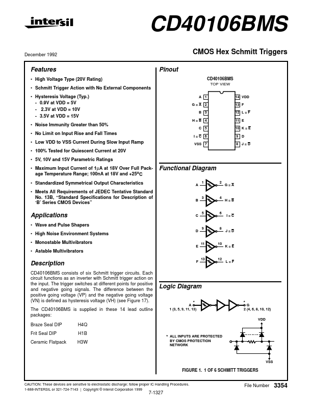
CD40106BMS consists of six Schmitt trigger circuits.
Key Features
- High Voltage Type (20V Rating)
- Hysteresis Voltage (Typ.) - 0.9V at VDD = 5V - 2.3V at VDD = 10V - 3.5V at VDD = 15V
- Noise Immunity Greater than 50%
- No Limit on Input Rise and Fall Times
- Low VDD to VSS Current During Slow Input Ramp
- 100% Tested for Quiescent Current at 20V
- Maximum Input Current of 1µA at 18V Over Full Package Temperature Range; 100nA at 18V and +25oC
- Standardized Symmetrical Output Characteristics
- Meets All Requirements of JEDEC Tentative Standard No. 13B, “Standard Specifications for Description of ‘B’ Series CMOS Devices”
Applications
- Wave and Pulse Shapers