CD40107BMS Overview
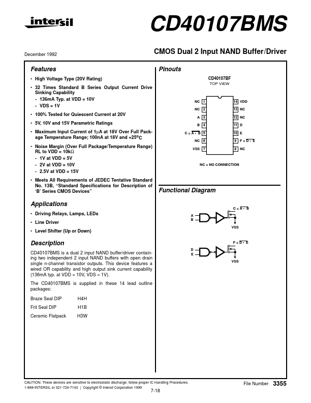
Description
CD40107BMS is a dual 2 input NAND buffer/driver containing two independent 2 input NAND buffers with open drain single n-channel transistor outputs. This device features a wired OR capability and high output sink current capability (136mA typ.
Key Features
- High Voltage Type (20V Rating)
- 32 Times Standard B Series Output Current Drive Sinking Capability
- 136mA Typ. at VDD = 10V
- 100% Tested for Quiescent Current at 20V
- 5V, 10V and 15V Parametric Ratings
- Maximum Input Current of 1µA at 18V Over Full Package Temperature Range; 100nA at 18V and +25oC
- Noise Margin (Over Full Package/Temperature Range) RL to VDD = 10kΩ
- 1V at VDD = 5V
- 2V at VDD = 10V
- 2.5V at VDD = 15V