CD4012BMS
Overview
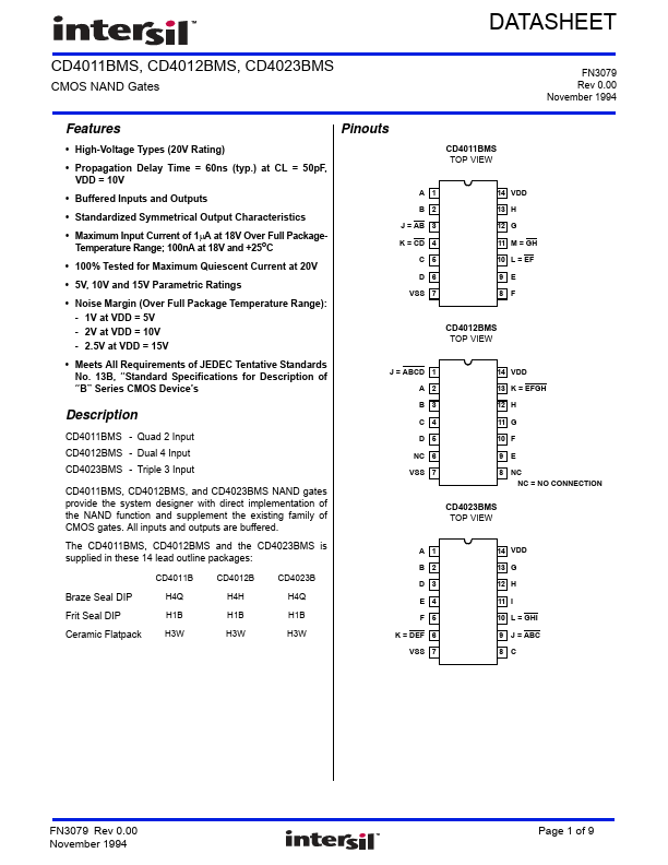
CD4011BMS - Quad 2 Input CD4012BMS - Dual 4 Input CD4023BMS - Triple 3 Input CD4011BMS, CD4012BMS, and CD4023BMS NAND gates provide the system designer with direct implementation of the NAND function and supplement the existing family of CMOS gates. All inputs and outputs are buffered.
- High-Voltage Types (20V Rating)
- Propagation Delay Time = 60ns (typ.) at CL = 50pF, VDD = 10V
- Buffered Inputs and Outputs
- Standardized Symmetrical Output Characteristics
- Maximum Input Current of 1µA at 18V Over Full PackageTemperature Range; 100nA at 18V and +25oC
- 100% Tested for Maximum Quiescent Current at 20V
- 5V, 10V and 15V Parametric Ratings