- Part: CD4041UBMS
- Description: CMOS Quad True/Complement Buffer
- Manufacturer: Intersil
- Size: 105.80 KB
Overview
- High Voltage Type (20V Rating)
- Balanced Sink and Source Current; Approximately 4 Times Standard “B” Drive
- Equalized Delay to True and Complement Outputs
- 100% Tested for Quiescent Current at 20V
- Maximum Input Current of 1µA at 18V Over Full Package-Temperature Range; - 100nA at 18V and +25oC
- 5V, 10V and 15V Parametric Ratings
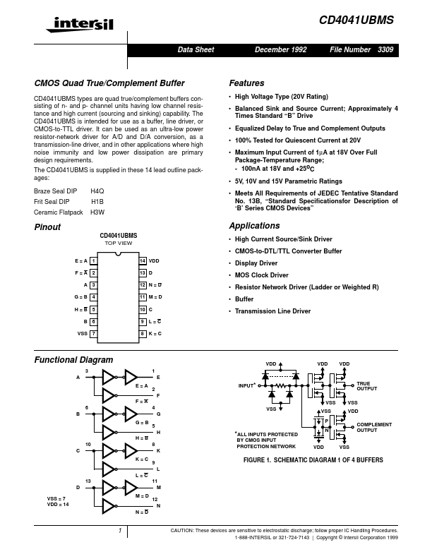
- Meets All Requirements of JEDEC Tentative Standard No. 13B, “Standard Specificationsfor Description of ‘B’ Series CMOS Devices” Pinout
Datasheets by Manufacturer
- CD4041UBM — Texas Instruments — CMOS QUAD TRUE/COMPLEMENT BUFFER
- CD4041UBE — Texas Instruments — CMOS QUAD TRUE/COMPLEMENT BUFFER
- CD4041UBF — Texas Instruments — CMOS QUAD TRUE/COMPLEMENT BUFFER
- CD4041UB — Texas Instruments — CMOS QUAD TRUE/COMPLEMENT BUFFER
- CD4044B — RCA — CMOS QUAD 3-STATE R/S LATCHES
- CD4042B — RCA — Quad Clocked D-Latch
- CD4043A — RCA — CMOS QUAD 3-STATE R/S LATCHES
- CD4044A — RCA — CMOS QUAD 3-STATE R/S LATCHES
- CD4048A — RCA — CMOS Multifunction Expandable 8-Input Gate
- CD4045A — RCA — CMOS 21-STAGE COUNTER