CD4048BMS
Features
- High-Voltage Type (20V Rating)
- Three State Output
- Many Logic Functions Available in One Package
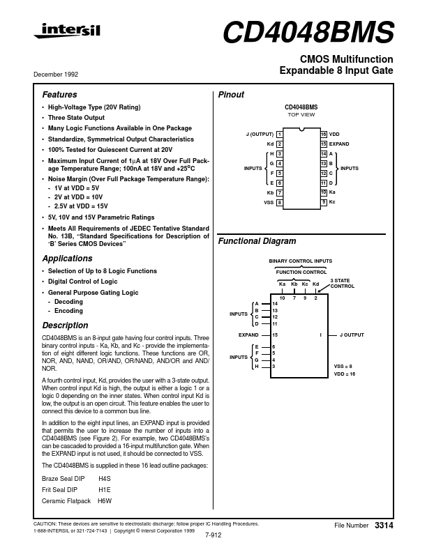
J (OUTPUT) 1
16 VDD 15 EXPAND 14 A 13 B INPUTS 12 C 11 D 10 Ka 9 Kc
- Standardize, Symmetrical Output Characteristics
- 100% Tested for Quiescent Current at 20V
- Maximum Input Current of 1µA at 18V Over Full Package Temperature Range; 100n A at 18V and +25o C
- Noise Margin (Over Full Package Temperature Range):
- 1V at VDD = 5V
- 2V at VDD = 10V
- 2.5V at VDD = 15V
- 5V, 10V and 15V Parametric Ratings
- Meets All Requirements of JEDEC Tentative Standard No. 13B, “Standard Specifications for Description of ‘B’ Series CMOS Devices”
INPUTS
Kd 2 H 3 G 4 F 5 E 6 Kb 7 VSS 8
Functional Diagram
BINARY CONTROL INPUTS FUNCTION CONTROL Ka 10 INPUTS A B C D 14 13 12 11 15 6 5 4 3 I J OUTPUT Kb Kc Kd 7 9 2 3 STATE CONTROL
Applications
- Selection of Up to 8 Logic Functions
- Digital Control of Logic
- General Purpose Gating Logic
- Decoding
- Encoding
Description
CD4048BMS is an...