CD4060BMS
Overview
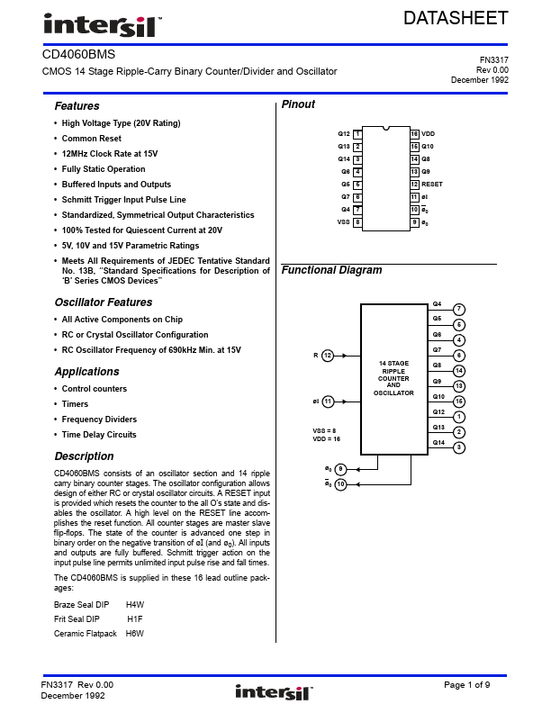
CD4060BMS consists of an oscillator s.
- High Voltage Type (20V Rating)
- Common Reset
- 12MHz Clock Rate at 15V
- Fully Static Operation
- Buffered Inputs and Outputs
- Schmitt Trigger Input Pulse Line
- Standardized, Symmetrical Output Characteristics
- 100% Tested for Quiescent Current at 20V
- 5V, 10V and 15V Parametric Ratings
- Meets All Requirements of JEDEC Tentative Standard No. 13B, “Standard Specifications for Description of ‘B’ Series CMOS Devices” Pinout