CD4068BMS Overview
Description
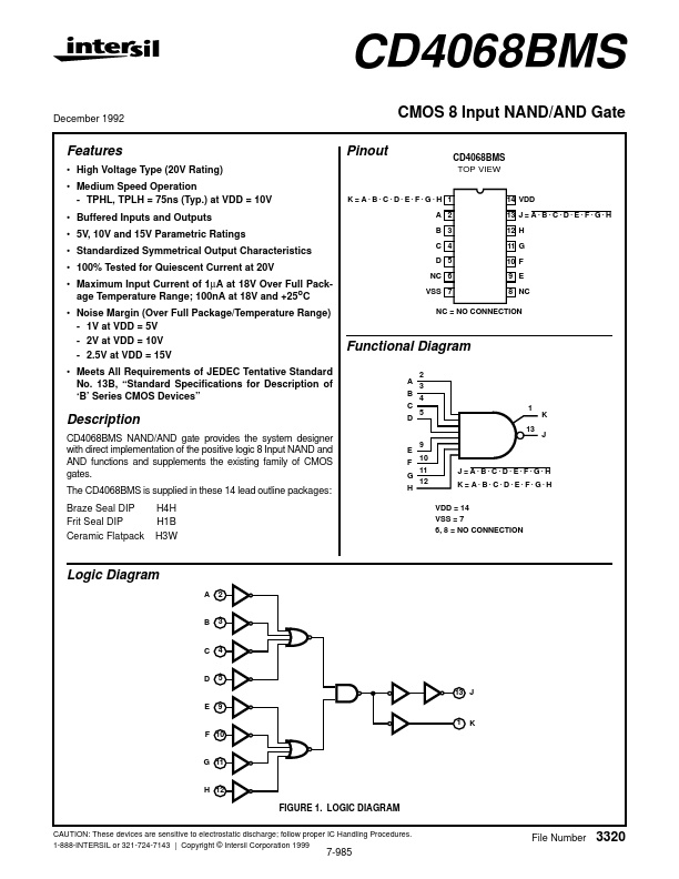
CD4068BMS NAND/AND gate provides the system designer with direct implementation of the positive logic 8 Input NAND and AND functions and supplements the existing family of CMOS gates. The CD4068BMS is supplied in these 14 lead outline packages: Braze Seal DIP Frit Seal DIP Ceramic Flatpack H4H H1B H3W Logic Diagram A 2 B 3 C 4 D 5 13 J E 9 1 K F 10 G 11 H 12 FIGURE 1.
Key Features
- High Voltage Type (20V Rating)
- Medium Speed Operation
- TPHL, TPLH = 75ns (Typ.) at VDD = 10V
- Buffered Inputs and Outputs
- 5V, 10V and 15V Parametric Ratings
- Standardized Symmetrical Output Characteristics
- 100% Tested for Quiescent Current at 20V
- Maximum Input Current of 1µA at 18V Over Full Package Temperature Range; 100nA at 18V and +25oC
- Noise Margin (Over Full Package/Temperature Range)
- 1V at VDD = 5V