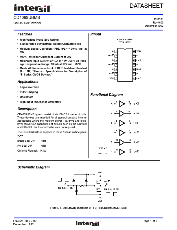
Datasheet4U Logo Datasheet4U.com

CD4069UBMS - CMOS Hex Inverter

General Description

of ‘B’ Series CMOS Devices” Applications A1 G=A 2 B3 H=B 4 C5 I=C 6 VSS 7 14 VDD 13 F 12 L = F 11 E 10 K = E 9D 8 J=D Logic Inversion Pulse Shaping Oscillators Functional Diagram High-Input-Impedance Amplifiers 1 A 2 G=A Description CD4069UBMS types c

Key Features

  • Pinout.
  • High Voltage Types (20V Rating).
  • Standardized Symmetrical Output Characteristics CD4069UBMS TOP VIEW.
  • Medium Speed Operation: tPHL, tPLH = 30ns (typ) at 10V.
  • 100% Tested for Quiescent Current at 20V.
  • Maximum Input Current of 1A at 18V Over Full Pack- age Temperature Range; 100nA at 18V and +25oC.
  • Meets All Requirements of JEDEC Tentative Standard No. 13B, “Standard Specifications for.

📥 Download Datasheet

Full PDF Text Transcription (Reference)

The following content is an automatically extracted verbatim text from the original manufacturer datasheet and is provided for reference purposes only.

View original datasheet text
DATASHEET CD4069UBMS CMOS Hex Inverter FN3321 Rev 0.00 December 1992 Features Pinout • High Voltage Types (20V Rating) • Standardized Symmetrical Output Characteristics CD4069UBMS TOP VIEW • Medium Speed Operation: tPHL, tPLH = 30ns (typ) at 10V • 100% Tested for Quiescent Current at 20V • Maximum Input Current of 1A at 18V Over Full Pack- age Temperature Range; 100nA at 18V and +25oC • Meets All Requirements of JEDEC Tentative Standard No.