CD4076BMS Overview
Description
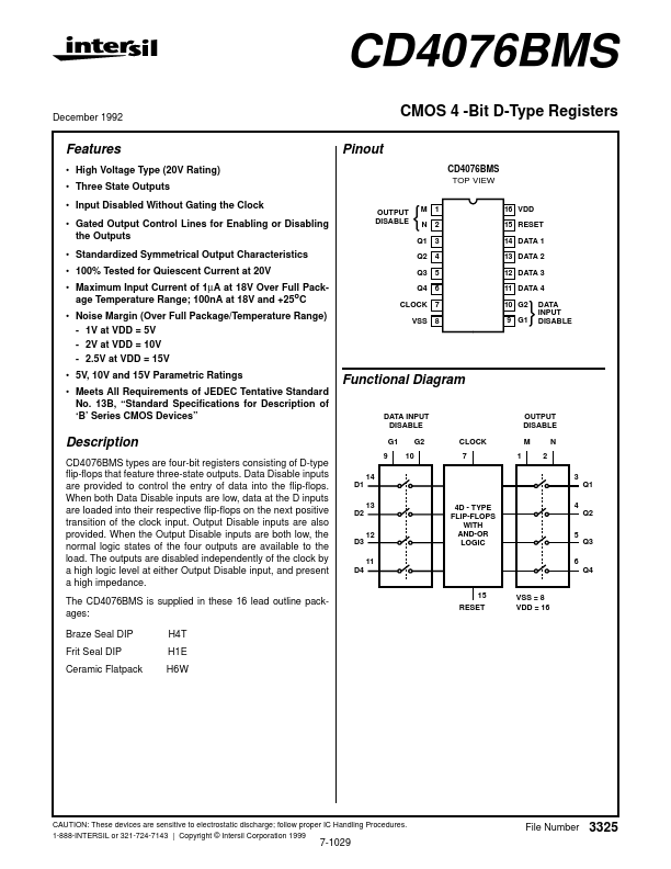
CD4076BMS types are four-bit registers consisting of D-type flip-flops that feature three-state outputs. Data Disable inputs are provided to control the entry of data into the flip-flops.
Key Features
- High Voltage Type (20V Rating)
- Three State Outputs
- Input Disabled Without Gating the Clock
- Gated Output Control Lines for Enabling or Disabling the Outputs
- Standardized Symmetrical Output Characteristics
- 100% Tested for Quiescent Current at 20V
- Maximum Input Current of 1µA at 18V Over Full Package Temperature Range; 100nA at 18V and +25oC
- Noise Margin (Over Full Package/Temperature Range)
- 1V at VDD = 5V
- 2V at VDD = 10V