Datasheet4U Logo Datasheet4U.com

CD4504BMS - CMOS Hex Voltage Level Shifter for TTL-to-CMOS or CMOS-to-CMOS Operation

General Description

of ‘B’ Series CMOS Devices” VCC 1 16 VDD 15 FOUT 14 FIN 13 SELECT 12 EOUT 11 EIN 10 DOUT 9 DIN AOUT 2 AIN BOUT BIN COUT CIN VSS 3 4 5 6 7 8 Functional Diagram VCC VDD LEVEL SHIFTER OUT (2, 4, 6, 10, 12, 15) Description 
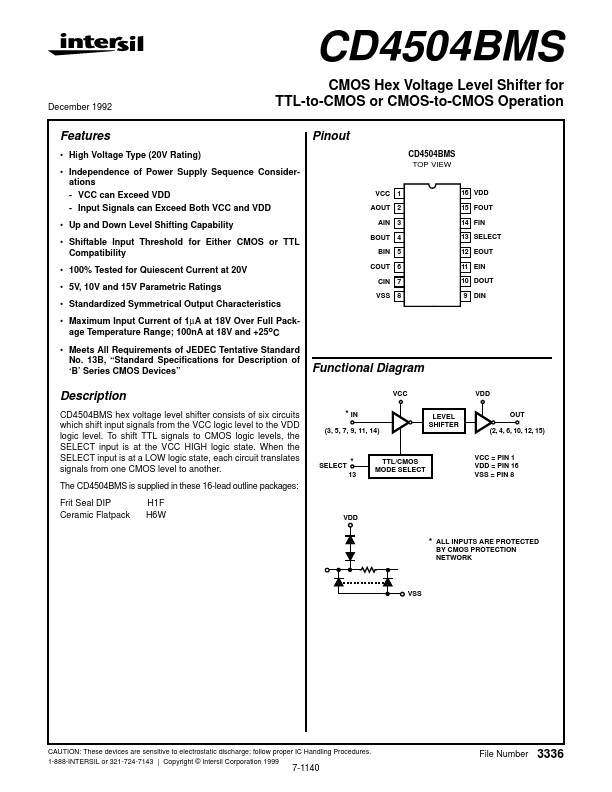
CD4504BMS hex voltage level shifter consists of six circuits which shift in

Key Features

  • High Voltage Type (20V Rating).
  • Independence of Power Supply Sequence Considerations - VCC can Exceed VDD - Input Signals can Exceed Both VCC and VDD.
  • Up and Down Level Shifting Capability.
  • Shiftable Input Threshold for Either CMOS or TTL Compatibility.
  • 100% Tested for Quiescent Current at 20V.
  • 5V, 10V and 15V Parametric Ratings.
  • Standardized Symmetrical Output Characteristics.
  • Maximum Input Current of 1µA at 18V Over Full.

📥 Download Datasheet

Full PDF Text Transcription (Reference)

The following content is an automatically extracted verbatim text from the original manufacturer datasheet and is provided for reference purposes only.

View original datasheet text
CD4504BMS December 1992 CMOS Hex Voltage Level Shifter for TTL-to-CMOS or CMOS-to-CMOS Operation Pinout CD4504BMS TOP VIEW Features • High Voltage Type (20V Rating) • Independence of Power Supply Sequence Considerations - VCC can Exceed VDD - Input Signals can Exceed Both VCC and VDD • Up and Down Level Shifting Capability • Shiftable Input Threshold for Either CMOS or TTL Compatibility • 100% Tested for Quiescent Current at 20V • 5V, 10V and 15V Parametric Ratings • Standardized Symmetrical Output Characteristics • Maximum Input Current of 1µA at 18V Over Full Package Temperature Range; 100nA at 18V and +25oC • Meets All Requirements of JEDEC Tentative Standard No.