CD4514BMS
Description
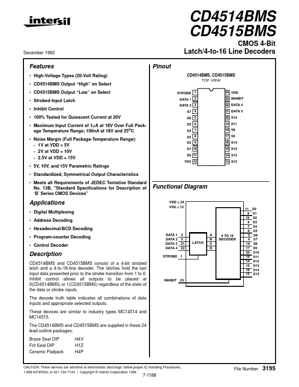
CD4514BMS and CD4515BMS consist of a 4-bit strobed latch and a 4-to-16-line decoder. The latches hold the last input data presented prior to the strobe transition from 1 to 0.
Key Features
- High-Voltage Types (20-Volt Rating)
- CD4514BMS Output “High” on Select
- CD4515BMS Output “Low” on Select
- Strobed Input Latch
- Inhibit Control
- 100% Tested for Quiescent Current at 20V
- Maximum Input Current of 1µA at 18V Over Full Package Temperature Range; 100nA at 18V and 25oC
- Noise Margin (Full Package-Temperature Range): - 1V at VDD = 5V - 2V at VDD = 10V - 2.5V at VDD = 15V
- 5V, 10V, and 15V Parametric Ratings
- Standardized, Symmetrical Output Characteristics