CD4520BMS
CD4520BMS is CMOS Dual Up Counters manufactured by Intersil.
CD4518BMS, CD4520BMS
December 1992
CMOS Dual Up Counters
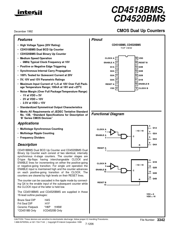
Pinout
CD4518BMS, CD4520BMS TOP VIEW
Features
- High Voltage Types (20V Rating)
- CD4518BMS Dual BCD Up Counter
- CD4520BMS Dual Binary Up Counter
- Medium Speed Operation
- 6MHz Typical Clock Frequency at 10V
- Positive or Negative Edge Triggering
- Synchronous Internal Carry Propagation
- 100% Tested for Quiescent Current at 20V
- 5V, 10V and 15V Parametric Ratings
- Maximum Input Current of 1µA at 18V Over Full Package Temperature Range; 100nA at 18V and +25oC
- Noise Margin (Over Full Package/Temperature Range)
- 1V at VDD = 5V
- 2V at VDD = 10V
- 2.5V at VDD = 15V
- Standardized Symmetrical Output Characteristics
- Meets All...