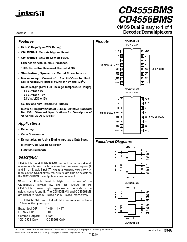
Description
of ‘B’ Series CMOS Devices”
1/2 OF DUAL
CD4555BMS TOP VIEW
E A B Q0 Q1 Q2 Q3 VSS 1 2 3 4 5 6 7 8 16 VDD 15 E 14 A 13 B 12 Q0 11 Q1 10 Q2 9 Q3 1/2 OF DUAL
Applications
Decoding
Code Conversion
Demultiplexing (Using Enable Input as a Data Input
Memory Chip-Ena
Features
- High Voltage Type (20V Rating).
- CD4555BMS: Outputs High on Select.
- CD4556BMS: Outputs Low on Select.
- Expandable with Multiple Packages
CD4556BMS TOP VIEW
16 VDD 15 E 14 A 13 B 12 Q0 11 Q1 10 Q2 9 Q3 1/2 OF DUAL
1/2 OF DUAL
Q0 Q1 Q2 Q3 VSS.
- 100% Tested for Quiescent Current at 20V.
- Standardized, Symmetrical Output Characteristics.
- Maximum Input Current of 1µA at 18V Over Full Package Temperature Range; 100nA at 18V and +25oC.