Datasheet Summary
December 1992
CMOS 4-Bit Magnitude parator
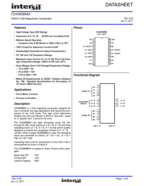
Pinout
CD4585BMS TOP VIEW
B2 A2 (A = B)OUT (A > B)IN (A < B)IN 1 2 3 4 5 6 7 8 16 VDD 15 A3 14 B3 13 (A > B)OUT 12 (A < B)OUT 11 B0 10 A0 9 B1
Features
- High Voltage Type (20V Rating)
- Expansion to 8, 12, 16 . . .4N Bits by Cascading Units
- Medium Speed Operation
- pares Two 4-Bit Words in 180ns (Typ.) at 10V
- 100% Tested for Quiescent Current at 20V
- Standardized Symmetrical Output Characteristics
- 5V, 10V and 15V Parametric Ratings
- Maximum Input Current of 1µA at 18V Over Full Package Temperature Range; 100nA at 18V and +25oC
- Noise Margin (Over Full Package/Temperature Range)
- 1V at VDD = 5V
- 2V at VDD = 10V
- 2.5V...