HI3197
HI3197 is 125 MSPS D/A Converter manufactured by Intersil.
Data Sheet October 1998 File Number 4356.1
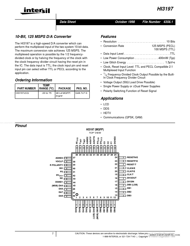
10-Bit, 125 MSPS D/A Converter
The HI3197 is a high-speed D/A converter which can perform the multiplexed input of the two system 10-bit data. The maximum conversion rate achieves 125 MSPS. The multiplexed operation is possible by the 1/2 frequencydivided clock or by halving the frequency of the clock with the clock frequency divider circuit having the reset pin in the IC. The data input is TTL; the clock input pin and reset input pin can select either TTL or PECL according to the application.
Features
- Resolution
- -
- -
- - . 10 Bits
- Conversion Rate 125 MSPS (PECL) 100 MSPS (TTL)
-...