Intersil ADC0803
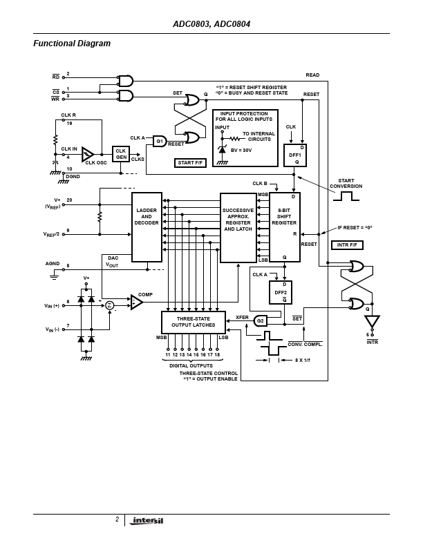
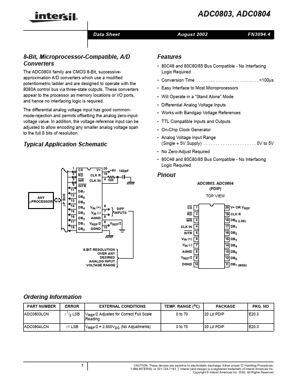
The ADC080X family are CMOS 8-Bit, successiveapproximation A/D converters which use a modified potentiometric ladder and are designed to operate with the 8080A control bus via three-state outputs. These converters appear to the processor as memory locations or I/O ports, and hence no interfacing logic is required. The differential analog voltage input has good commonmode-rejection and permits offsetting the analog zero-inputvoltage value.| Part No. | ADC0803 |
|---|---|
| Datasheet | ADC0803 Download |
| Manufacturer |  Intersil |
| Description | A/D Converters |
| Buy | Stock & Price |
FEATURES
● 80C48 and 80C80/85 Bus Compatible - No Interfacing Logic Required● Conversion Time . . . . . . . . . . . . . . . . . . . . . . . . . . <100µs
● Easy Interface to Most Microprocessors
● Will Operate in a “Stand Alone” Mode
● Differential Analog Voltage Inputs
● Works with Bandgap Voltage References
● TTL Compatible Inputs and Outputs
● On-Chip Clock Generator
● Analog Voltage Input Range (Single + 5V Supply) . . . . . . . . . . . . . . . . . . . . . . 0V to 5V
● No Zero-Adjust Required
● 80C48 and 80C80/85 Bus Compatible - No Interfacing Logic Required Typical Application Schematic 1 2 3 5 11 µP BUS ANY µPROCESSOR 12 13 14 15 16 17 18 CS RD WR INTR DB7 DB6 DB5 DB4 DB3 DB2 DB1 DB0 V+ 20 +5V 150pF CLK R 19 CLK IN 4 10K Pinout ADC0803, ADC0804 (PDIP) TOP VIEW VIN (+) 6 V (-) 7 AGND 8 /2 9 V DGND 10 REF IN DIFF INPUTS VREF/2 CS RD WR CLK IN INTR VIN (+) VIN (-) 1 2 3 4 5 6 7 8 9 20 V+ OR VREF 19 CLK R 18 DB0 (LSB) 17 DB1 16 DB2 15 DB3 14 DB4 13 DB5 12 DB6 11 DB7 (MSB) 8-BIT RESO...