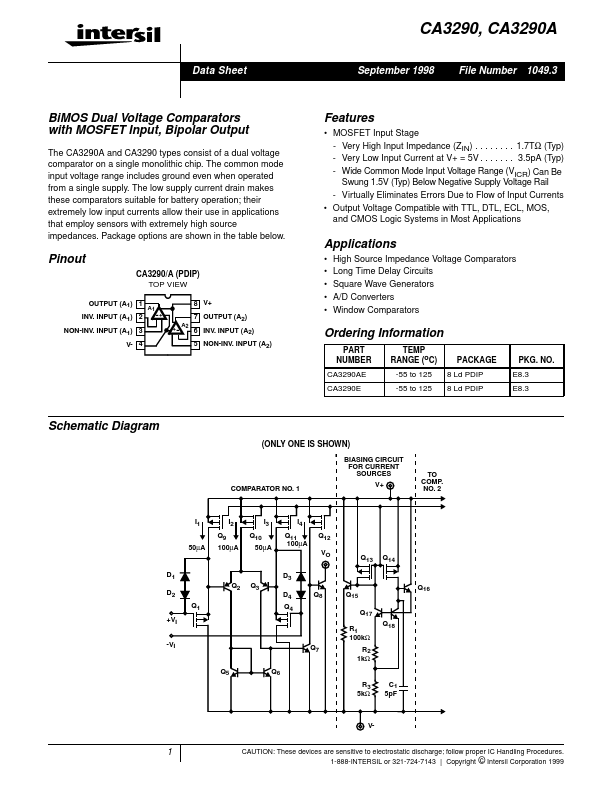
Datasheet4U Logo Datasheet4U.com

CA3290 - BiMOS Dual Voltage Comparators

General Description

Figure 4 shows the basic circuit diagram for one of the two comparators in the CA3290.

It is generically similar to the industry type “139” comparators, with PMOS transistors replacing PNP transistors as input stage elements.

Key Features

  • MOSFET Input Stage - Very High Input Impedance (ZIN).
  • . . . 1.7TΩ (Typ) - Very Low Input Current at V+ = 5V.
  • . . 3.5pA (Typ) - Wide Common Mode Input Voltage Range (VICR) Can Be Swung 1.5V (Typ) Below Negative Supply Voltage Rail - Virtually Eliminates Errors Due to Flow of Input Currents.
  • Output Voltage Compatible with TTL, DTL, ECL, MOS, and CMOS Logic Systems in Most.

📥 Download Datasheet

Full PDF Text Transcription (Reference)

The following content is an automatically extracted verbatim text from the original manufacturer datasheet and is provided for reference purposes only.

View original datasheet text
CA3290, CA3290A Data Sheet September 1998 File Number 1049.3 BiMOS Dual Voltage Comparators with MOSFET Input, Bipolar Output The CA3290A and CA3290 types consist of a dual voltage comparator on a single monolithic chip. The common mode input voltage range includes ground even when operated from a single supply. The low supply current drain makes these comparators suitable for battery operation; their extremely low input currents allow their use in applications that employ sensors with extremely high source impedances. Package options are shown in the table below. Features • MOSFET Input Stage - Very High Input Impedance (ZIN) . . . . . . . . 1.7TΩ (Typ) - Very Low Input Current at V+ = 5V . . . . . . . 3.5pA (Typ) - Wide Common Mode Input Voltage Range (VICR) Can Be Swung 1.