Intersil CD4007UBMS
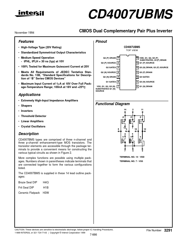
The CD4007BMS is supplied in these 14 lead outline packages: Braze Seal DIP Frit Seal DIP Ceramic Flatpack H4Q H1B H3W 7 4 9 TERMINAL NO.| Part No. | CD4007UBMS |
|---|---|
| Datasheet | CD4007UBMS Download |
| Manufacturer |  Intersil |
| Description | CMOS Dual Complementary Pair Plus Inverter |
| Buy | Stock & Price |
FEATURES
● High-Voltage Type (20V Rating)● Standardized Symmetrical Output Characteristics
● Medium Speed Operation - tPHL, tPLH = 30 ns (typ) at 10V
● 100% Tested for Maximum Quiescent Current at 20V
● Meets All Requirements of JEDEC Tentative Standards No. 13B, “Standard Specifications for
DESCRIPTION
of “B” Series CMOS Devices”● Maximum Input Current of 1µA at 18V Over Full Package-Temperature Range; 100nA at 18V and +25oC 14 VDD, Q1, Q2, Q3 (P) SUBSTRATES, Q1(P) DRAIN 13 Q1 (P) SOURCE 12 Q3 (N) DRAIN, Q3 (P) SOURCE 11 Q3 (P) DRAIN 10 Q3 GATES 9 Q3 (N) SOURCE 8 Q1 (N) DRAIN 7
APPLICATIONS
● Extremely High-Input Impedance Amplifiers● Shapers
● Inverters
● Threshold Detector
● Linear Amplifiers
● Crystal Oscillators 6 13 8 n n 3 1 5 n 10 12 Functional Diagram 14 2 11 p p p
DESCRIPTION
CD4007BMS types are comprised of three n-channel and three p-channel enhancement-type MOS transistors. The transistor elements are accessible through the package terminals to provide a convenient means for constructing the various typical circuits as shown in Figure 2.