Intersil CD40104BMS
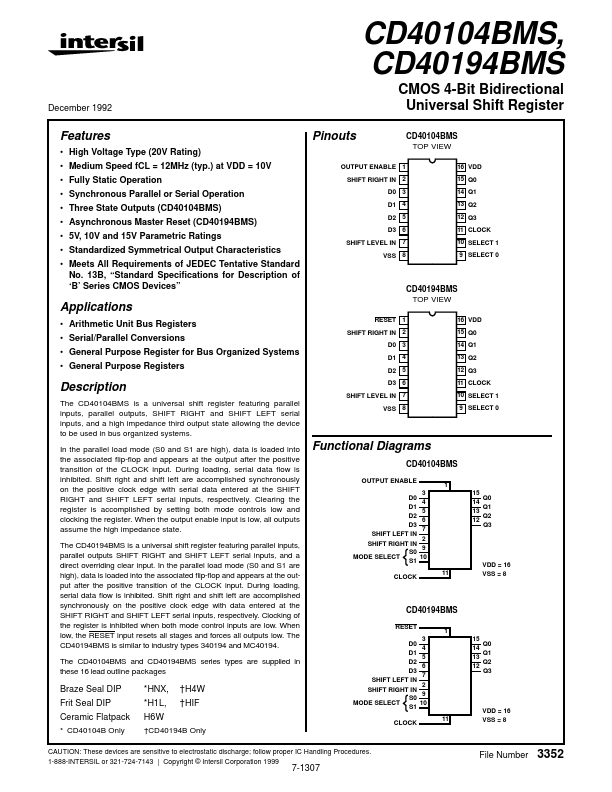
The CD40104BMS is a universal shift register featuring parallel inputs, parallel outputs, SHIFT RIGHT and SHIFT LEFT serial inputs, and a high impedance third output state allowing the device to be used in bus organized systems. The CD40104BMS and CD40194BMS series types are supplied in these 16 lead outline packages Functional Diagrams CD40104BMS OUTPUT ENABLE D0 D1 D2 D3 SHIFT LEFT IN SHIFT RIGHT IN S0 MODE SELECT S1 CLOCK 3 4 5 6 7 2 9 10 11 1 15 Q0 14 Q1 13 Q2 12 Q3 VDD = 16 VSS = 8 CD40194BMS RESET D0 D1 D2 D3 SHIFT...| Part No. | CD40104BMS |
|---|---|
| Datasheet | CD40104BMS Download |
| Manufacturer |  Intersil |
| Description | CMOS 4-Bit Bidirectional Universal Shift Register |
| Buy | Stock & Price |
FEATURES
● High Voltage Type (20V Rating)● Medium Speed fCL = 12MHz (typ.) at VDD = 10V
● Fully Static Operation
● Synchronous Parallel or Serial Operation
● Three State Outputs (CD40104BMS)
● Asynchronous Master Reset (CD40194BMS)
● 5V, 10V and 15V Parametric Ratings
● Standardized Symmetrical Output Characteristics
● Meets All Requirements of JEDEC Tentative Standard No. 13B, “Standard Specifications for
DESCRIPTION
of ‘B’ Series CMOS Devices” CD40104BMS TOP VIEW 16 VDD 15 Q0 14 Q1 13 Q2 12 Q3 11 CLOCK 10 SELECT 1 9 SELECT 0APPLICATIONS
● Arithmetic Unit Bus Registers● Serial/Parallel Conversions
● General Purpose Register for Bus Organized Systems
● General Purpose Registers RESET 1 SHIFT RIGHT IN 2 D0 3 D1 4 D2 5 D3 6 SHIFT LEVEL IN 7 VSS 8 CD40194BMS TOP VIEW 16 VDD 15 Q0 14 Q1 13 Q2 12 Q3 11 CLOCK 10 SELECT 1 9 SELECT 0
DESCRIPTION
In the parallel load mode (S0 and S1 are high), data is loaded into the associated flip-flop and appears at the output after the positive transition of the CLOCK input.