Intersil CD4043BMS
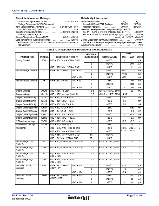
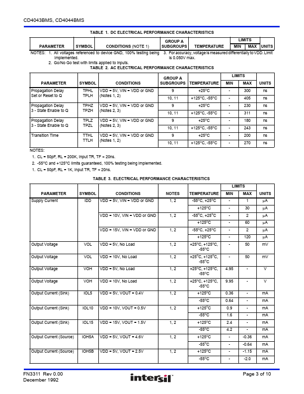
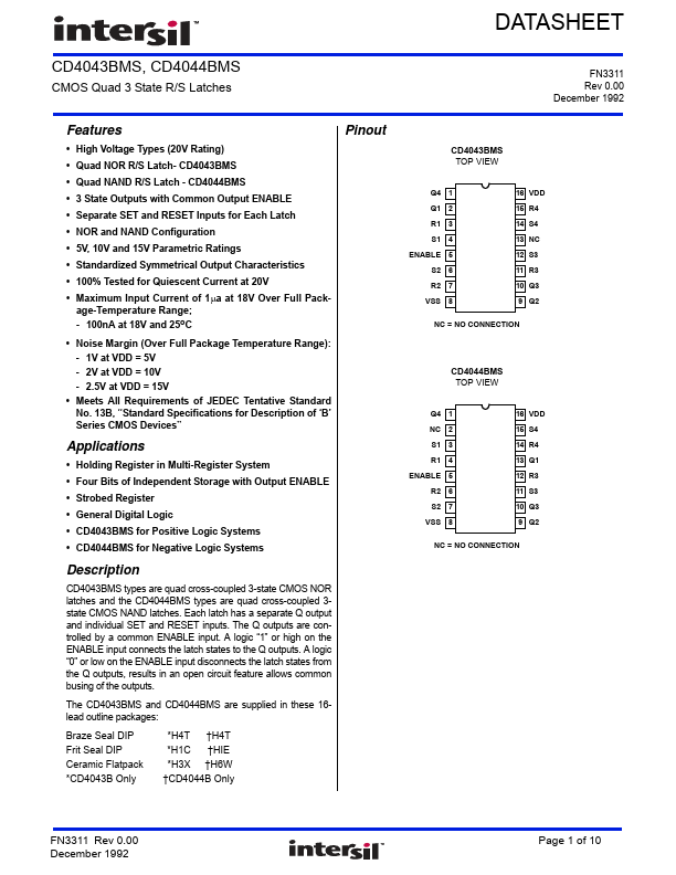
The CD4043BMS and CD4044BMS are supplied in these 16lead outline packages: Braze Seal DIP Frit Seal DIP Ceramic Flatpack *CD4043B Only *H4T †H4T *H1C †HIE *H3X †H6W †CD4044B Only CD4043BMS TOP VIEW Q4 1 Q1 2 R1 3 S1 4 ENABLE 5 S2 6 R2 7 VSS 8 16 VDD 15 R4 14 S4 13 NC 12 S3 11 R3 10 Q3 9 Q2 NC = NO CONNECTION CD4044BMS TOP VIEW Q4 1 NC 2 S1 3 R1 4 ENABLE 5 R2 6 S2 7 VSS 8 16 VDD 15 S4 14 R4 13 Q1 12 R3 11 S3 10 Q3 9 Q2 NC = NO CONNECTION FN3311 Rev 0.00 December 1992 Page 1 of 10 CD4043BMS, CD4044BMS Absolute Maximum Ratings DC Supply Voltage Range, (VDD) .| Part No. | CD4043BMS |
|---|---|
| Datasheet | CD4043BMS Download |
| Manufacturer |  Intersil |
| Description | CMOS Quad 3 State R/S Latche |
| Buy | Stock & Price |
FEATURES
● High Voltage Types (20V Rating)● Quad NOR R/S Latch- CD4043BMS
● Quad NAND R/S Latch - CD4044BMS
● 3 State Outputs with Common Output ENABLE
● Separate SET and RESET Inputs for Each Latch
● NOR and NAND Configuration
● 5V, 10V and 15V Parametric Ratings
● Standardized Symmetrical Output Characteristics
● 100% Tested for Quiescent Current at 20V
● Maximum Input Current of 1a at 18V Over Full Package-Temperature Range; - 100nA at 18V and 25oC
● Noise Margin (Over Full Package Temperature Range): - 1V at VDD = 5V - 2V at VDD = 10V - 2.5V at VDD = 15V
● Meets All Requirements of JEDEC Tentative Standard No. 13B, “Standard Specifications for
DESCRIPTION
of ‘B’ Series CMOS Devices” PinoutAPPLICATIONS
● Holding Register in Multi-Register System● Four Bits of Independent Storage with Output ENABLE
● Strobed Register
● General Digital Logic
● CD4043BMS for Positive Logic Systems
● CD4044BMS for Negative Logic Systems
DESCRIPTION
CD4043BMS types are quad cross-coupled 3-state CMOS NOR latches and the CD4044BMS types are quad cross-coupled 3state CMOS NAND latches.