Intersil CD4502BMS
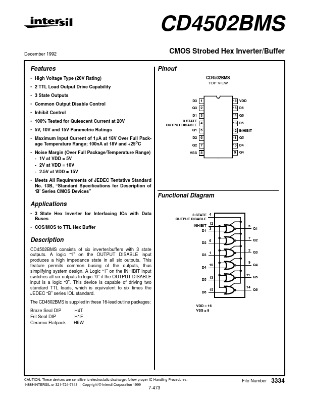
The CD4502BMS is supplied in these 16-lead outline packages: Braze Seal DIP Frit Seal DIP Ceramic Flatpack H4T H1F H6W D3 1 2 Q3 D4 10 9 Q4 D5 13 11 Q5 D6 15 14 Q6 VDD = 16 VSS = 8 CAUTION: These devices are sensitive to electrostatic discharge; follow proper IC Handling Procedures.| Part No. | CD4502BMS |
|---|---|
| Datasheet | CD4502BMS Download |
| Manufacturer |  Intersil |
| Description | CMOS Strobed Hex Inverter/Buffer |
| Buy | Stock & Price |
FEATURES
● High Voltage Type (20V Rating)● 2 TTL Load Output Drive Capability
● 3 State Outputs
● Common Output Disable Control
● Inhibit Control
● 100% Tested for Quiescent Current at 20V
● 5V, 10V and 15V Parametric Ratings
● Maximum Input Current of 1µA at 18V Over Full Package Temperature Range; 100nA at 18V and +25oC
● Noise Margin (Over Full Package/Temperature Range) - 1V at VDD = 5V - 2V at VDD = 10V - 2.5V at VDD = 15V
● Meets All Requirements of JEDEC Tentative Standard No. 13B, “Standard Specifications for
DESCRIPTION
of ‘B’ Series CMOS Devices” D3 Q3 D1 1 2 3 16 VDD 15 D6 14 Q6 13 D5 12 INHIBIT 11 Q5 10 D4 9 Q4 3 STATE 4 OUTPUT DISABLE Q1 5 D2 Q2 VSS 6 7 8 Functional Diagram 3 STATE 4 OUTPUT DISABLE 12 INHIBIT 3 D1 D2 6APPLICATIONS
● 3 State Hex Inverter for Interfacing ICs with Data Buses● COS/MOS to TTL Hex Buffer 5 7 Q1 Q2
DESCRIPTION
CD4502BMS consists of six inverter/buffers with 3 state outputs. A logic “1” on the OUTPUT DISABLE input produces a high impedance state in all six outputs.
