Intersil DG308A
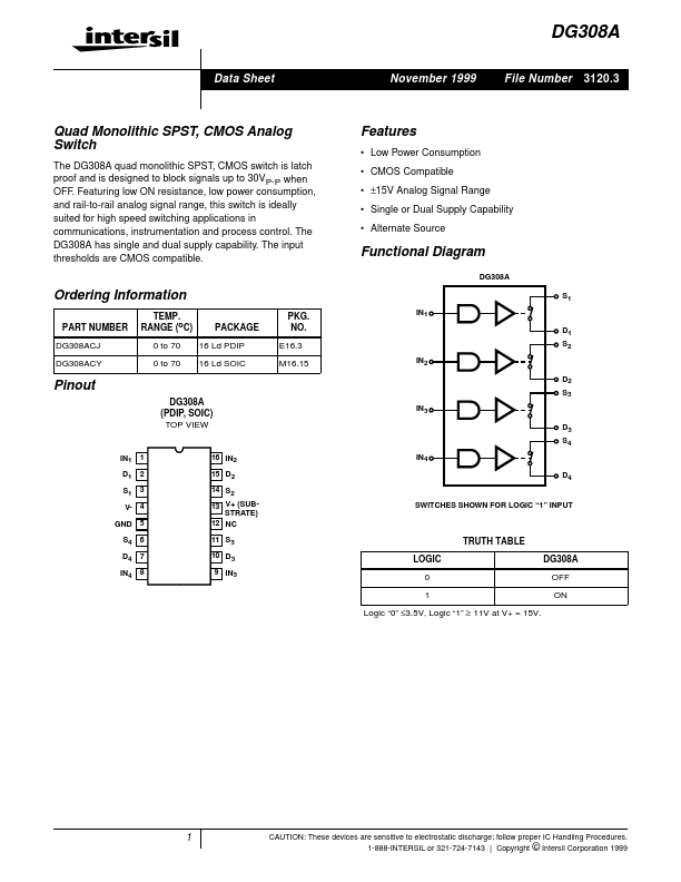
The DG308A quad monolithic SPST, CMOS switch is latch proof and is designed to block signals up to 30VP-P when OFF. Featuring low ON resistance, low power consumption, and rail-to-rail analog signal range, this switch is ideally suited for high speed switching applications in communications, instrumentation and process control. The DG308A has single and dual supply capability.| Part No. | DG308A |
|---|---|
| Datasheet | DG308A Download |
| Manufacturer |  Intersil |
| Description | Quad Monolithic SPST / CMOS Analog Switch |
| Buy | Stock & Price |
FEATURES
● Low Power Consumption● CMOS Compatible
● ±15V Analog Signal Range
● Single or Dual Supply Capability
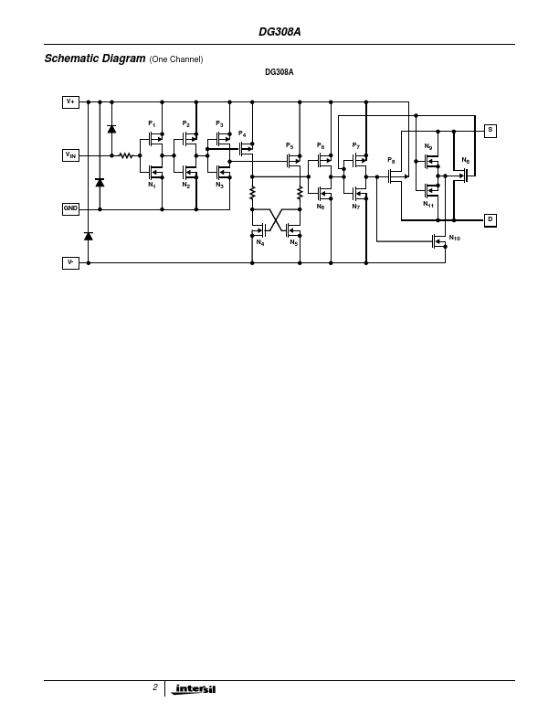
● Alternate Source Functional Diagram DG308A Ordering Information PART NUMBER DG308ACJ DG308ACY TEMP. RANGE (oC) 0 to 70 0 to 70 PACKAGE 16 Ld PDIP 16 Ld SOIC PKG. NO. E16.3 M16.15 IN2 IN1 S1 D1 S2 Pinout DG308A (PDIP, SOIC) TOP VIEW IN3 D2 S3 D3 S4 IN1 D1 S1 VGND S4 D4 IN4 1 2 3 4 5 6 7 8 - 16 IN2 15 D2 14 S2 13 V+ (SUBSTRATE) 12 NC 11 S3 10 D3 9 IN3 IN4 D4 SWITCHES SHOWN FOR LOGIC “1” INPUT TRUTH TABLE LOGIC 0 1 Logic “0” ≤3.5V, Logic “1” ≥ 11V at V+ = 15V. DG308A OFF ON 1 CAUTION: These devices are sensitive to electrostatic discharge; follow proper IC Handling Procedures. 1-888-INTERSIL or 321-724-7143 | Copyright © Intersil Corporation 1999 DG308A Schematic Diagram (One Channel) DG308A V+ P1 P2 P3 P4 P5 P6 P7 P8 N9 N8 S VIN N1 GND N2 N3 N6 N7 N11 D N10 N4 V- N5 2 DG308A
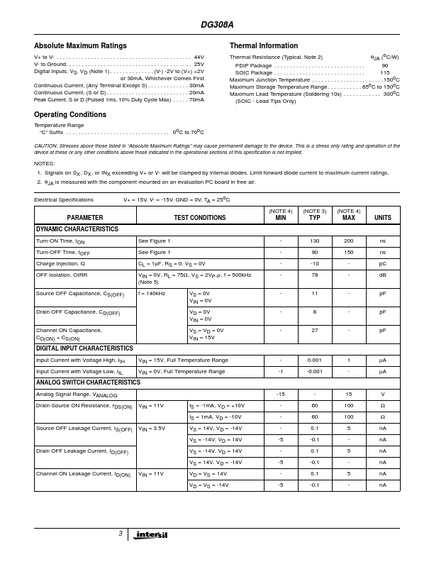
ABSOLUTE MAXIMUM RATINGS
V+ to V- . . . . . . . . . . . . . . . . . . . . . . . . . . . . . . . . . . . . . . . . . . .