Intersil DG406
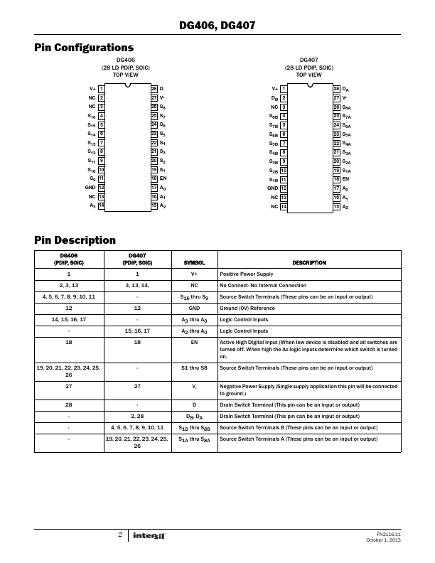
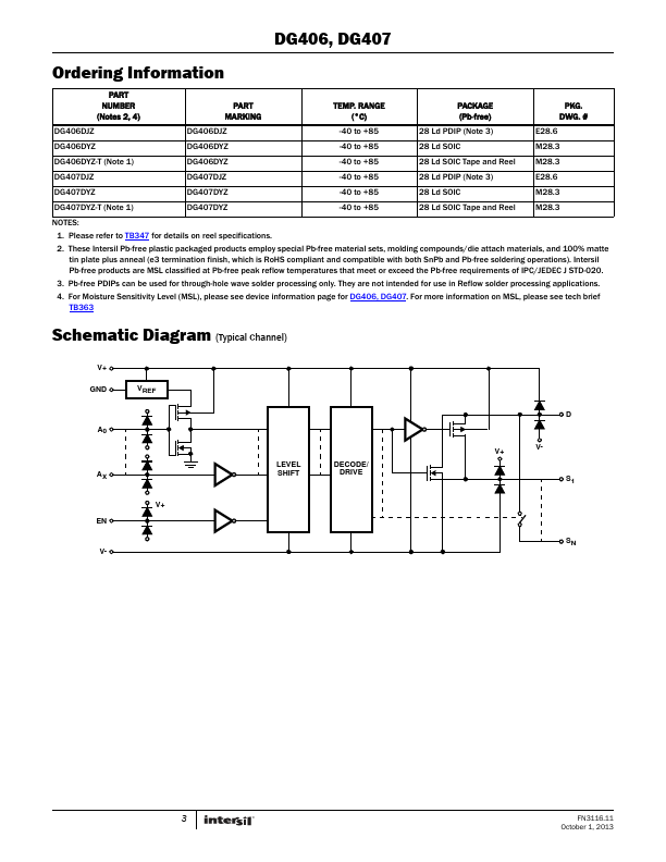
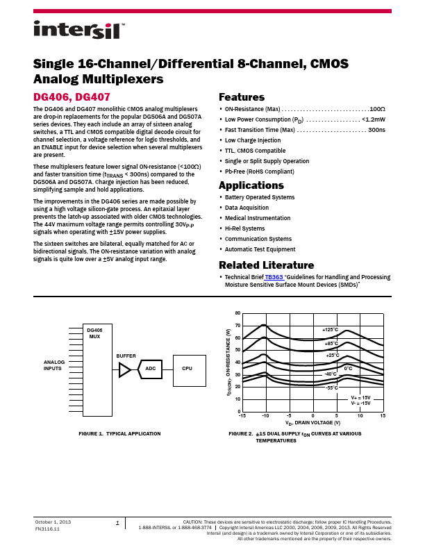
The DG406 and DG407 monolithic CMOS analog multiplexers are drop-in replacements for the popular DG506A and DG507A series devices. They each include an array of sixteen analog switches, a TTL and CMOS compatible digital decode circuit for channel selection, a voltage reference for logic thresholds, and an ENABLE input for device selection when several multiplexers are present. These multiplexers feature lower signal ON-resistance (| Part No. | DG406 |
|---|---|
| Datasheet | DG406 Download |
| Manufacturer |  Intersil |
| Description | CMOS Analog Multiplexers |
| Buy | Stock & Price |
FEATURES
● ON-Resistance (Max) . . . . . . . . . . . . . . . . . . . . . . . . . . . . .100Ω● Low Power Consumption (PD) . . . . . . . . . . . . . . . . . . <1.2mW
● Fast Transition Time (Max) . . . . . . . . . . . . . . . . . . . . . . . 300ns
● Low Charge Injection
● TTL, CMOS Compatible
● Single or Split Supply Operation
● Pb-Free (RoHS Compliant)
APPLICATIONS
● Battery Operated Systems● Data Acquisition
● Medical Instrumentation
● Hi-Rel Systems
● Communication Systems
● Automatic Test Equipment Related Literature
● Technical Brief TB363 “Guidelines for Handling and Processing Moisture Sensitive Surface Mount Devices (SMDs)” ANALOG INPUTS DG406 MUX BUFFER ADC CPU FIGURE 1. TYPICAL APPLICATION rDS(ON), ON-RESISTANCE (W) 80 70 +125°C 60 +85°C 50 +25°C 40 0°C 30 -40°C 20 -55°C 10 V+ = 15V V- = -15V 0 -15 -10 -5 0 5 10 VD , DRAIN VOLTAGE (V) FIGURE 2. ±15 DUAL SUPPLY rON CURVES AT VARIOUS TEMPERATURES 15 October 1, 2013 FN3116.11 1 CAUTION: These devices are sensitive to electrostatic discharge; follow proper IC Handling Procedures.