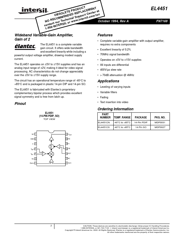
Description
MIN TYP VDIFF Signal input differential input voltage Clipping 0.2% nonlinearity 1.8 2.0 1.3 VCM VOS VOS, FB VG, 100% VG, 0% VG, 1V IB IOS NL Ft RIN, VIN RIN, FB RIN, RGAIN CMRR PSRR VO ISC IS mon-mode range of VIN; VDIFF = 0, Input offset voltage VS = ±5V VS = ±15V Output offset voltage Extrapolated voltage for 100% gain Extrapolated voltage for 0% gain Gain at VGAIN = 1V Input bias current (all inputs) Input offset current between VIN +and VIN-, Gain+ and Gain-, FB and Ref Nonlinearity, VIN between -1V and +1V, VG = 1V Signal feedthrough, VG = -1V Input resistance, VIN Input resistance, FB Input resistance, gain input mon-mode rejection ratio of VIN Power supply rejection ratio of VOS, FB, VS = ±5V to ±15V Output voltage swing (VIN = 0, VREF varied) VS = ±5V VS = ±15V Output s.
Key Features
- Excellent linearity of 0.2%
- 70MHz signal bandwidth
- Operates on ±5V to ±15V supplies
- All inputs are differential
- 400V/µs slew rate
- > 70dB attenuation @ 4MHz