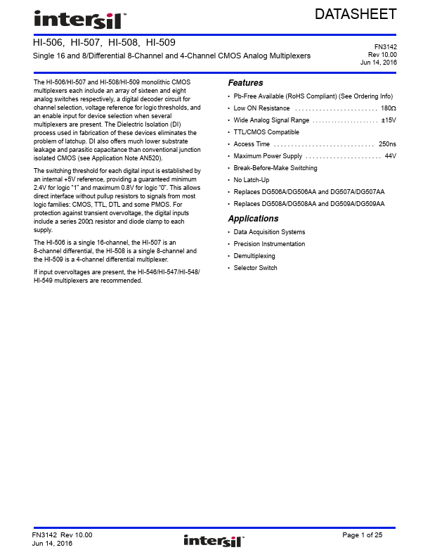
| Part | HI-509 |
|---|---|
| Description | CMOS Analog Multiplexer |
| Manufacturer | Intersil |
| Size | 0.99 MB |
Related Datasheets
| Part Number | Manufacturer | Description |
|---|---|---|
| HI-509A | Renesas | CMOS Analog MUX |
| HI-506A | Harris Corporation | CMOS Analog MUXs |
| HI-509A | Harris Corporation | CMOS Analog MUXs |
| HI-508A | Harris Corporation | CMOS Analog MUXs |
| HI-507A | Harris Corporation | CMOS Analog MUXs |


