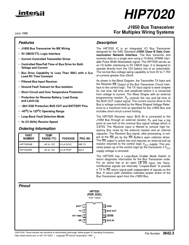
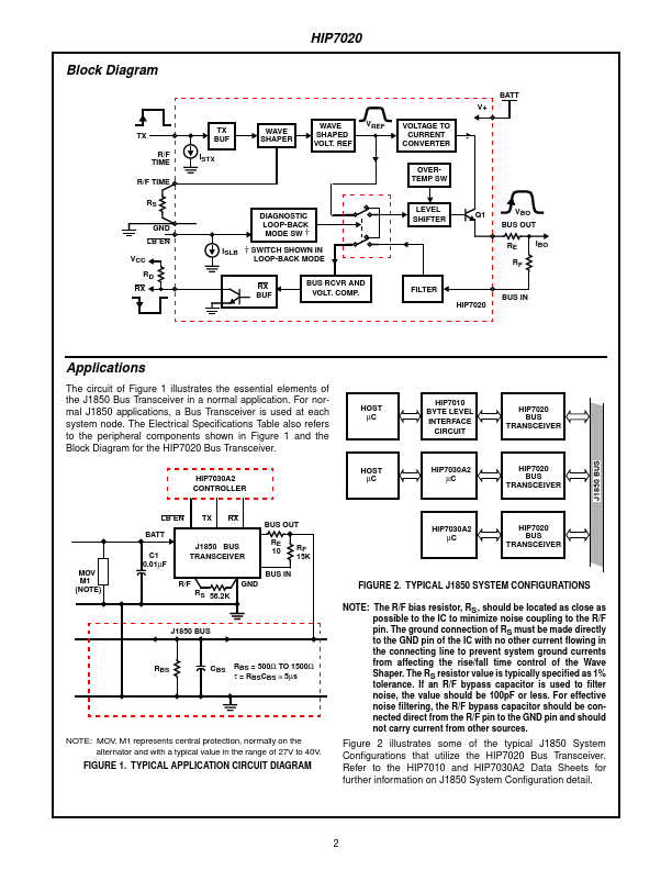
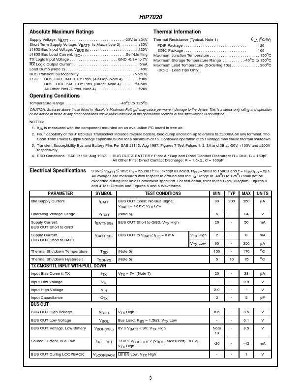
DESCRIPTION
It is designed to operate directly from the 12V battery line of an automobile. The normal Bus voltage swing capability is from 0V to 7.75V at currents greater than 20mA. As shown in the Block Diagram, the Transmitter TX Input and the Receiver RX Output of the Bus Transceiver Circuit interface to the control logic. The TX input signal is wave shaped for rise time, fall time and amplitude before it is converted from voltage to current. The Wave Shaper with an external programming resistor, RS controls the rise and fall time of the BUS OUT output signal. The current source drive to the Bus is voltage controlled by the Wave Shaped Voltage Reference to a maximum limit as specified for the J1850 Bus and includes short-circuit current limiting. The HIP7020 Receiver input, BUS IN is connected to the J1850 Bus through an external resistor, RF and has a trip point at one-half of the nominal Bus signal voltage which is 3.875V. The Receiver input is filtered to remove high frequency Bus noise by the external resistor and an internal capacitor. Intersil