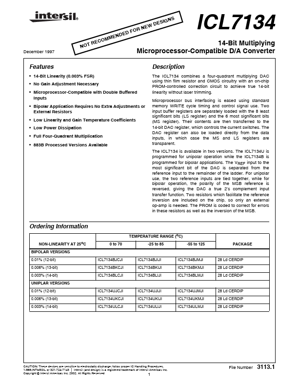
DESCRIPTION
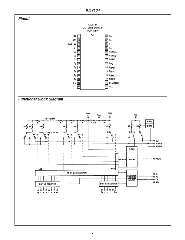
Microprocessor bus interfacing is eased using standard memory WRITE cycle timing and control signal use. Two input buffer registers are separately loaded with the 8 least significant bits (LS register) and the 6 most significant bits (MS register). Their contents are then transferred to the 14-bit DAC register, which controls the current switches. The ICL7134 is available in two versions. The ICL7134U is programmed for unipolar operation while the ICL7134B is programmed for bipolar applications. The VREF input to the most significant bit of the DAC is separated from the reference input to the remainder of the ladder. For unipolar use, the two reference inputs are tied together, while for bipolar operation, the polarity of the MSB reference is reversed, giving the DAC a true 2’s complement input transfer function. Two resistors which facilitate the reference inversion are included on the chip, so only an external op-amp is needed. The PROM is coded to correct for errors in these resistors as well as the inversion of the MSB. Intersil