ISL22326WM Overview
Key Specifications
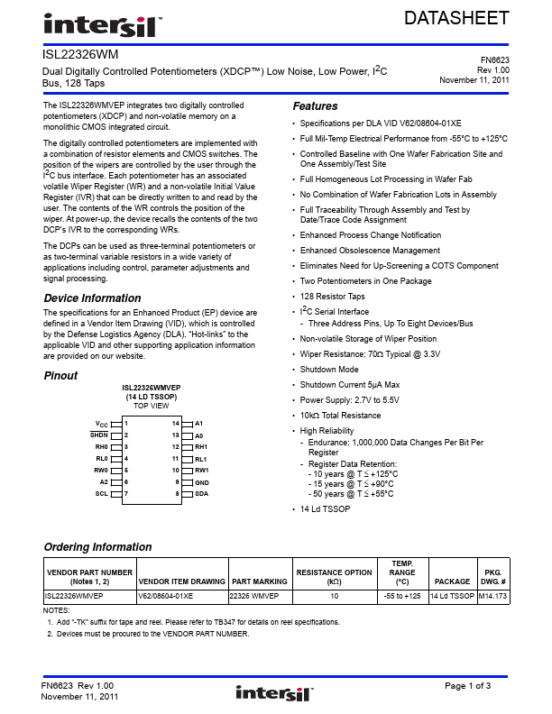
Package: TSSOP
Mount Type: Surface Mount
Pins: 14
Operating Voltage: 3.3 V
Key Features
- Specifications per DLA VID V62/08604-01XE
- Full Mil-Temp Electrical Performance from -55°C to +125°C
- Controlled Baseline with One Wafer Fabrication Site and One Assembly/Test Site
- Full Homogeneous Lot Processing in Wafer Fab
- No Combination of Wafer Fabrication Lots in Assembly