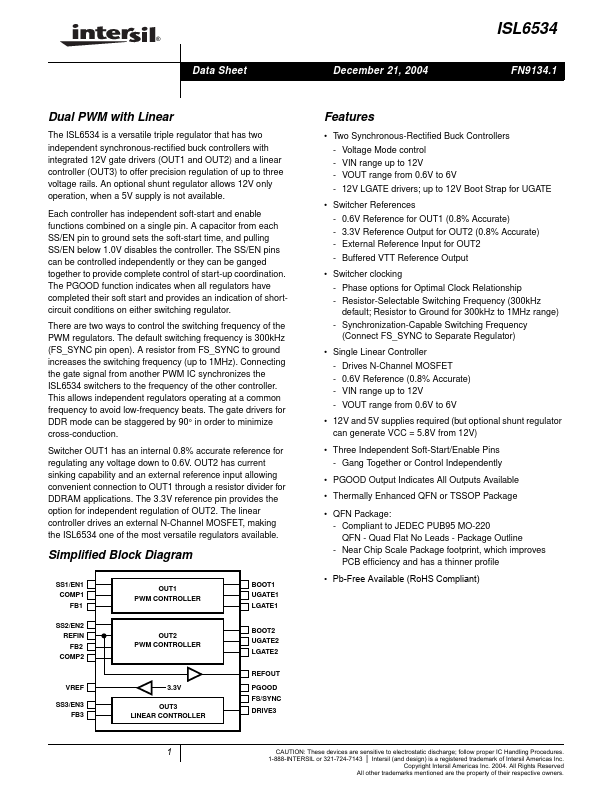
ISL6534 Overview
| Part | ISL6534 |
|---|---|
| Description | Dual PWM |
| Manufacturer | Intersil |
| Size | 600.15 KB |
| Part Number | Manufacturer | Description |
|---|---|---|
| 6534CV | Intersil | ISL6534CV |
| ISL6534 | Renesas | Dual PWM |
| ISL6536 | Renesas | Four Channel Supervisory IC |
| ISL6532A | Renesas | ACPI Regulator/Controller |
| ISL6531 | Renesas | Dual 5V Synchronous Buck Pulse-Width Modulator (PWM) Controller |