Datasheet Summary
December 1992
CMOS 4 -Bit D-Type Registers
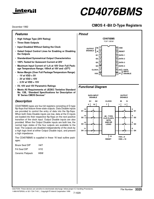
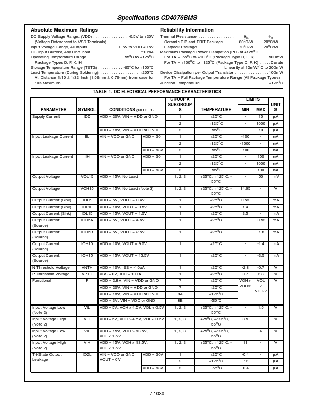
Pinout
CD4076BMS TOP VIEW
M N Q1 Q2 Q3 Q4 CLOCK VSS 1 2 3 4 5 6 7 8 16 VDD 15 RESET 14 DATA 1 13 DATA 2 12 DATA 3 11 DATA 4 10 G2 9 G1 DATA INPUT DISABLE
Features
- High Voltage Type (20V Rating)
- Three State Outputs
- Input Disabled Without Gating the Clock
- Gated Output Control Lines for Enabling or Disabling the Outputs
- Standardized Symmetrical Output Characteristics
- 100% Tested for Quiescent Current at 20V
- Maximum Input Current of 1µA at 18V Over Full Package Temperature Range; 100nA at 18V and +25oC
- Noise Margin (Over Full Package/Temperature Range)
- 1V at VDD = 5V
- 2V at VDD = 10V
- 2.5V at VDD = 15V
- 5V, 10V and 15V...