DESCRIPTION
Single-ended clock and data inputs eliminate the need for phase-matched traces, simplifying the board layout. The clock input and duobinary output are AC-coupled in the package. The data input should be ACcoupled outside the package. The device is housed in a rugged, RoHS-6-compliant, ceramic package. Compact duobinary conversion and transmitter drive functions Supports external Bessel filter and pre-filtered modulator applications Adjustable AC coupled output voltage from 6.0 to 10.5 Vpp Power dissipation: 3.3 W with +8 V and -5 V supply voltages Single-ended, AC-coupled data and clock inputs RoHS-6-compliant, 7x8 mm2 (0.278 x 0.315 mil2) SMT ceramic package with bottom pad grounding and heat sinking -5V Supply FEATURES
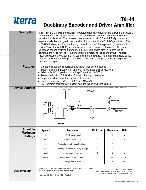
Device Diagram 13dB 13dB Vadj ABSOLUTE MAXIMUM RATINGS
Symbol Vdd Vee Vg1 Vg2 Vadj Tbase Tst Parameter +8 VDC supply input -5 VDC supply input First gate negative supply voltage Second gate negative supply voltage Output voltage adjustment Base operating temperature Storage temperature Minimum Maximum 10 Unit V V -6 -2 -2 -3 0 0 +2 85 125 V V V o C oC This is a Production data sheet.