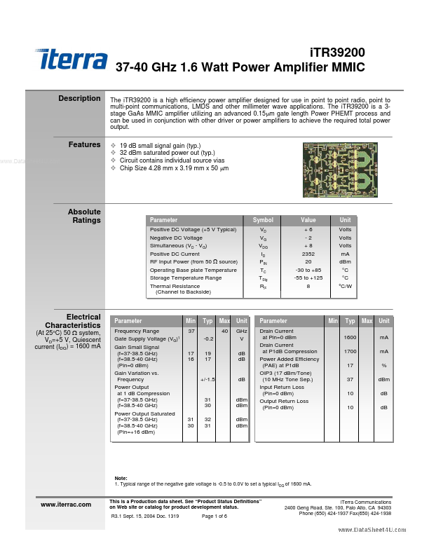
DESCRIPTION
19 dB small signal gain (typ.) 32 dBm saturated power out (typ.) Circuit contains individual source vias Chip Size 4.28 mm x 3.19 mm x 50 μm FEATURES
Absolute Ratings Parameter Positive DC Voltage (+5 V Typical) Negative DC Voltage Simultaneous (VD - VG) Positive DC Current RF Input Power (from 50 Ω source) Operating Base plate Temperature Storage Temperature Range Thermal Resistance (Channel to Backside) Symbol VD VG VDG ID PIN TC TStg Rjc Value +6 -2 +8 2352 20 -30 to +85 -55 to +125 8 Unit Volts Volts Volts mA dBm °C °C °C/W (At 25°C) 50 Ω system, VD=+5 V, Quiescent current (IDQ) = 1600 mA ELECTRICAL CHARACTERISTICS
Parameter Frequency Range Gate Supply Voltage (VG)1 Gain Small Signal (f=37-38.5 GHz) (f=38.5-40 GHz) (Pin=0 dBm) Gain Variation vs. Frequency Power Output at 1 dB Compression (f=37-38.5 GHz) (f=38.5-40 GHz) Power Output Saturated (f=37-38.5 GHz) (f=38.5-40 GHz) (Pin=+16 dBm) Min 37 Typ -0.2 Max 40 Unit GHz V dB dB Parameter Drain Current at Pin=0 dBm...