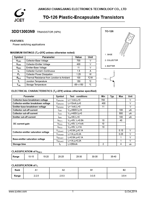
3DD13003N9
FEATURES
Power switching applications
MAXIMUM RATINGS (Ta=25℃ unless otherwise noted)
Symbol
Parameter
Value
VCBO VCEO VEBO
IC PC RθJA Tj Tstg
Collector-Base Voltage Collector-Emitter Voltage Emitter-Base Voltage Collector Current -Continuous Collector Power Dissipation Thermal Resistance from Junction to Ambient Junction Temperature Storage Temperature
700 400 11 1.5 1.25 100 150 -55~+150
Unit
V V V A W ℃/W ℃ ℃
ELECTRICAL CHARACTERISTICS (Ta=25℃ unless otherwise specified)
Parameter Collector-base breakdown voltage Collector-emitter breakdown voltage Emitter-base breakdown voltage Collector cut-off current Collector cut-off current Emitter cut-off current
DC current gain
Collector-emitter saturation voltage
Base-emitter saturation voltage Storage time
Symbol
Test conditions
V(B=R)CBO IC= 1m A,IE 0 V(BR=)CEO IC=10m A,IB 0 V(=BR)EBO IE=...