CJ3400A
FEATURE
APPLICATION z High dense cell design for extremely low RDS(ON) z Load/Power Switching z Exceptional on-resistance and maximum DC current capability z Interfacing Switching
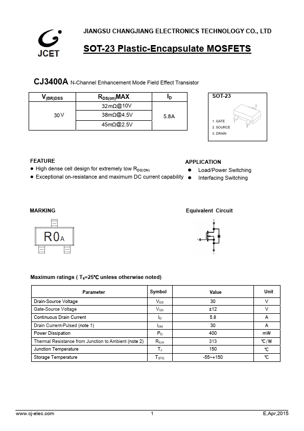
MARKING
Equivalent Circuit
Maximum ratings ( Ta=25℃ unless otherwise noted)
Parameter Drain-Source Voltage Gate-Source Voltage Continuous Drain Current Drain Current-Pulsed (note 1) Power Dissipation Thermal Resistance from Junction to Ambient (note 2) Junction Temperature Storage Temperature
Symbol VDS VGS ID IDM PD RθJA TJ TSTG
Value 30 ±12 5.8 30 400 313 150 -55~+150
Unit
V V A A m W ℃/W ℃ ℃
.cj-elec.
E,Apr,2015
MOSFET ELECTRICAL CHARACTERISTICS
Ta=25 ℃ unless otherwise specified
Parameter
Symbol
Test Condition
Off Characteristics
Drain-source breakdown voltage
V(BR) DSS VGS = 0V, ID =250µA
Zero gate voltage drain current
IDSS
VDS =24V,VGS = 0V
Gate-source leakage current
IGSS
VGS =±12V, VDS = 0V
On characteristics (note 3)
Drain-source on-resistance (note 3)
RDS(on)
VGS...