CJM3005
Overview
JIANGSU CHANGJIANG ELECTRONICS TECHNOLOGY CO., LTD DFNWB2X2-6L-J Plastic-Encapsulate MOSFETS CJM3005 N-Channel MOSFET V(BR)DSS RDS(on)MAX ID 42 mΩ@10V 30V 44 mΩ@4.5V 5A 50 mΩ@2.5V DFNWB2×2-6...
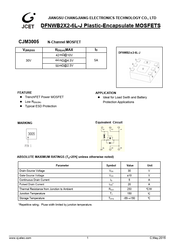
JIANGSU CHANGJIANG ELECTRONICS TECHNOLOGY CO., LTD DFNWB2X2-6L-J Plastic-Encapsulate MOSFETS CJM3005 N-Channel MOSFET V(BR)DSS RDS(on)MAX ID 42 mΩ@10V 30V 44 mΩ@4.5V 5A 50 mΩ@2.5V DFNWB2×2-6...