JCET EMD9
Digital Transistors
| Part No. | EMD9 |
|---|---|
| Datasheet | EMD9 Download |
| Manufacturer |  JCET |
| Description | Digital Transistors |
| Buy | Stock & Price |
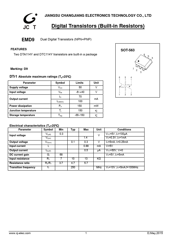
FEATURES
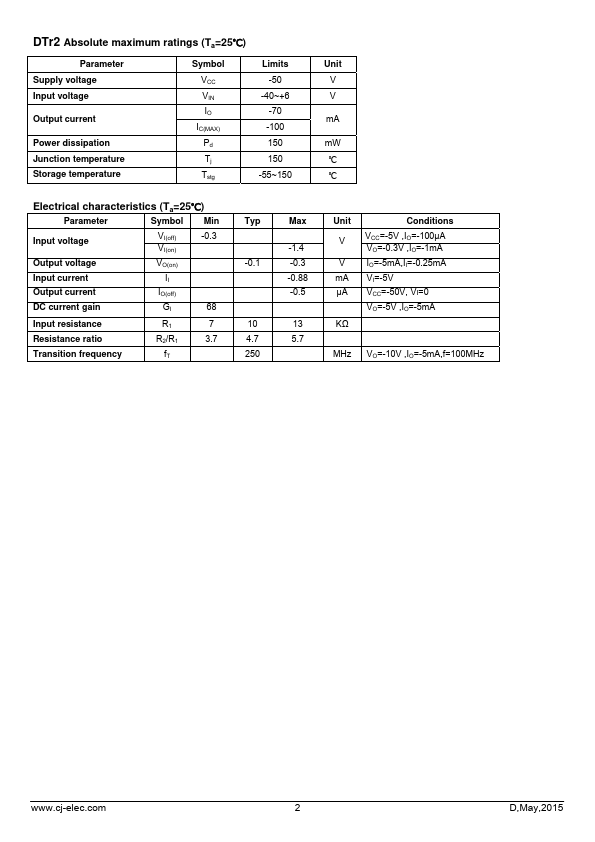
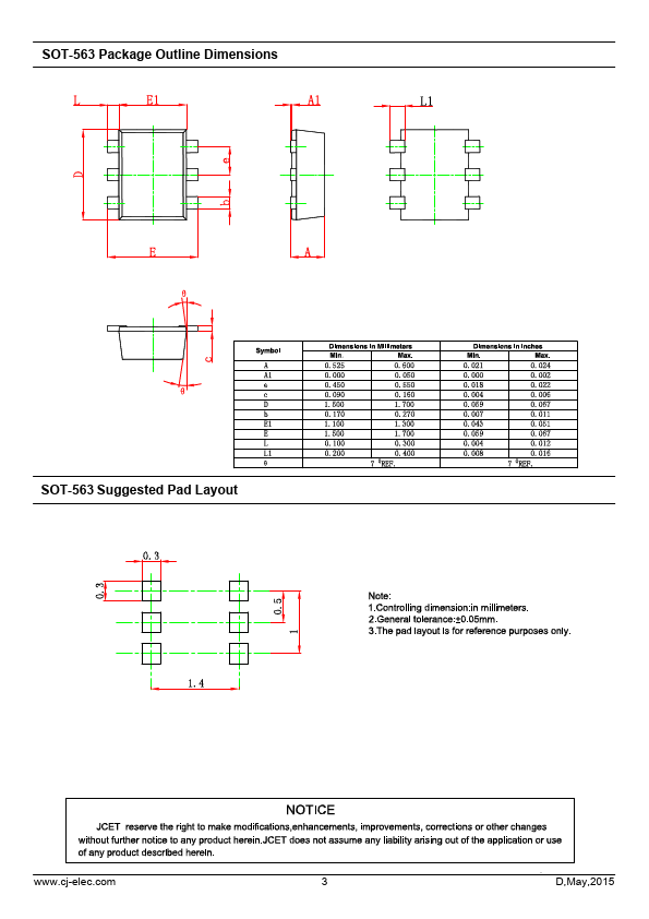
Two DTA114Y and DTC114Y transistors are built-in a package SOT-563 Marking: D9 DTr1 Absolute maximum ratings (Ta=25℃) Parameter Supply voltage Input voltage Output current Power dissipation Junction temperature Storage temperature Symbol VCC VIN IO IC(MAX) Pd Tj Tstg Limits 50 -6~+40 70 100 150 150 -55~150 Unit V V mA mW ℃ ℃ Electrical characteristics (Ta=25℃) Parameter Symbol Min Input voltage VI(off) VI(on) 0.3 Output voltage VO(on) Input current II Output current IO(off) DC current gain GI 68 Input resistance R1 7 Resistance ratio R2/R1 3.7 Transition frequency fT Typ 0.1 10 4.7 250 Max 1.4 0.3 0.88 0.5 13 5.7 Unit V V mA μA KΩ Conditions VCC=5V ,IO=100μA VO=0.3V ,IO=1mA IO=5mA, II=0.25mA VI=5V VCC=50V, VI=0 VO=5V ,IO=5mA MHz VO=10V ,IO=5mA,f=100MHz 1 D,May,2015 DTr2 Absolu