JCET MMBD4448
SWITCHING DIODE
| Part No. | MMBD4448 |
|---|---|
| Datasheet | MMBD4448 Download |
| Manufacturer |  JCET |
| Description | SWITCHING DIODE |
| Buy | Stock & Price |
FEATURES
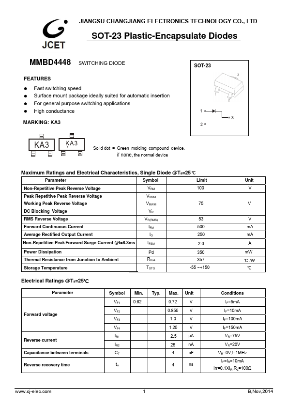
z Fast switching speed z Surface mount package ideally suited for automatic insertion z For general purpose switching applications z High conductance MARKING: KA3 SOT-23 1. A1NODE 2. N, C 3. C2ATHODE 3 KA3 KA3 Solid dot = Green molding compound device, if none, the normal deviceMAXIMUM RATINGS
andELECTRICAL CHARACTERISTICS
, Single Diode @Ta=25 ℃ Parameter Symbol Limit Non-Repetitive Peak Reverse Voltage VRM 100 Peak Repetitive Peak Reverse Voltage VRRM Working Peak Reverse Voltage VRWM 75 DC Blocking Voltage VR RMS Reverse Voltage VR(RMS) 53 Forward Continuous Current IFM 500 Average Rectified Output Current IO 250 Non-Repetitive Peak Forward Surge Current @t=8.3ms IFSM 2.0 Power Dissipation Thermal Resistance from Junction to Ambient Storage Temperature Pd RθJA TSTG 350 357 -55 ~+150 Unit V V V mA mA A mW ℃K/W ℃ Electrical Ratings @Ta=25℃ Parameter Forward voltage Reverse current Capacitance between terminals Reverse recovery time Symbol VF1 VF2 VF3 VF4 IR1 IR2 CT trr Min. 0.62 Typ.