JCST CJ2333
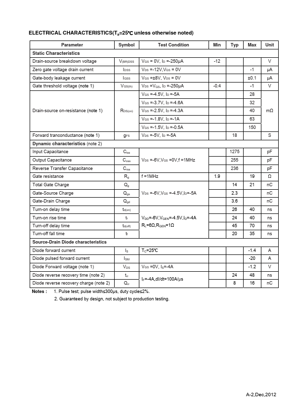
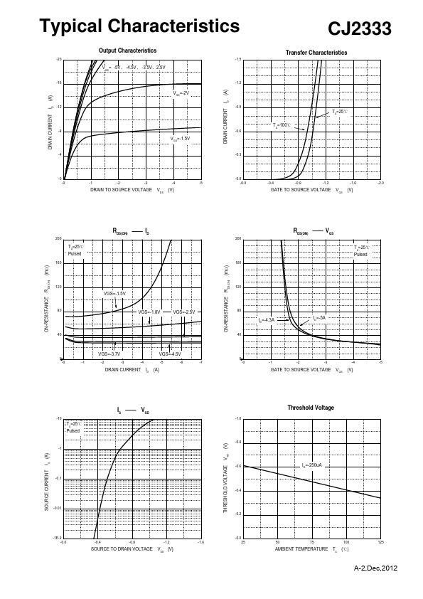
The CJ2333 uses advanced trench technology and design to provide excellent RDS(on) with low gate charge.This device is suitable for use in PWM,load switching and general purpose applications.| Part No. | CJ2333 |
|---|---|
| Datasheet | CJ2333 Download |
| Manufacturer |  JCST |
| Description | P-Channel MOSFET |
| Buy | Stock & Price |

DESCRIPTION
1. GATE 2. SOURCE 3. DRAIN FEATURE● TrenchFET Power MOSFET APPLICATION
● DC/DC Converter
● Load Switch for Portable Devices
● Battery Switch MARKING: S33
MAXIMUM RATINGS
(Ta=25℃ unless otherwise noted) Parameter Symbol Value Drain-Source Voltage Gate-Source Voltage Continuous Drain Current Pulsed Drain Current (t=300µs) Power Dissipation Thermal Resistance from Junction to Ambient VDS VGS ID IDM PD RθJA -12 ±8 -6 a -20 0.35 b 1.1a 357 b 113 a Junction Temperature Storage Temperature TJ TSTG 150 -55~ +150 a. Device mounted on FR-4 substrate board, with minimum recommended pad layout, single side. b. Device mounted on no heat sink. Unit V V