Datasheet Details
| Part number | CJ3420 |
|---|---|
| Manufacturer | JCST |
| File Size | 705.67 KB |
| Description | N-Channel Enhancement Mode Field Effect Transistor |
| Download | CJ3420 Download (PDF) |
|
|
|
| Part number | CJ3420 |
|---|---|
| Manufacturer | JCST |
| File Size | 705.67 KB |
| Description | N-Channel Enhancement Mode Field Effect Transistor |
| Download | CJ3420 Download (PDF) |
|
|
|
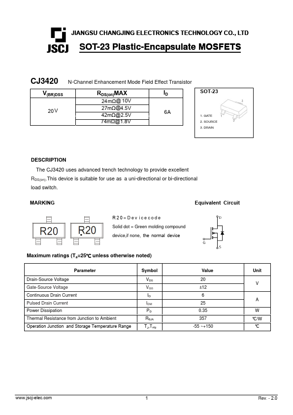
The CJ3420 uses advanced trench technology to provide excellent RDS(on).This device is suitable for use as a uni-directional or bi-directional load switch.
MARKING Equivalent Circuit R20=Dev icecode Solid dot = Green molding compound device,if none, the normal device Maximum ratings (Ta=25℃ unless otherwise noted) Parameter Drain-Source Voltage Gate-Source Voltage Continuous Drain Current Pulsed Drain Current Power Dissipation Thermal Resistance from Junction to Ambient Operation Junction and Storage Temperature Range Symbol VDS VGS ID IDM PD RθJA TJ,Tstg Value 20 ±12 6 25 0.35 357 -55 ~+150 Unit V A W ℃/W ℃ www.jscj-elec.com 1 Rev.
- 2.0 MOSFET ELECTRICAL CHARACTERISTICS Ta=25 ℃ unless otherwise specified Parameter Off Characteristics Drain-source breakdown voltage Symbol Test Condition V(BR) DSS VGS = 0V, ID =250µA Zero gate voltage drain current Gate-source leakage current IDSS VDS =16V,VGS = 0V,TJ=25℃ VDS =16V,VGS = 0V,T J=125℃ IGSS VGS =±12V, VDS = 0V On characteristics VGS =10V, ID =6A Drain-source on-resistance② RDS(on) VGS =4.5V, ID =5A VGS =2.5V, ID =4A VGS =1.8V, ID =2A Forward transconductance gFS VDS =5V, ID =3.8A Gate threshold voltage VGS(th) VDS =VGS, ID =250µA Dynamic Characteristics ③ Input capacitance Ciss Output capacitance Coss VDS =10V,VGS =0V,f =1MHz Reverse transfer capacitance Crss Gate resistance Rg VDS =0V,VGS =0V,f =1MHz Switching Characteristics ③ Turn-on delay time td(on) Turn-on rise time Turn-off delay time Turn-off fall time tr td(off) tf VGS= 10V,VDS= 15V, R=L 2.7Ω,RGEN= 3Ω Total Gate Charge Gate-Source Charge Gate-Drain Charge Qg Qgs VDS=10V,ID=6A, VGS=4.5V Qgd Drain-source diode characteristics and maximum rati
JIANGSU CHANGJING ELECTRONICS TECHNOLOGY CO., LTD SOT-23 Plastic-Encapsulate MOSFETS CJ3420 N-Channel Enhancement Mode Field Effect Transistor V(BR)DSS 20 V RDS(on)MAX ID 24mΩ@ 10V 27mΩ@4.5V 42mΩ@2.5V 6A 74mΩ@1.8V SOT-23 1.
GATE 2.
SOURCE 3.
| Part Number | Description |
|---|---|
| CJ3400 | N-Channel Enhancement Mode Field Effect Transistor |
| CJ3401 | MOSFETS |
| CJ3401A | MOSFETS |
| CJ3402 | MOSFETS |
| CJ3404 | MOSFETS |
| CJ3406 | MOSFETS |
| CJ3407 | MOSFETS |
| CJ3415 | P-Channel 20-V(D-S) MOSFET |
| CJ3439KDW | MOSFETS |
| CJ3134K | MOSFETS |