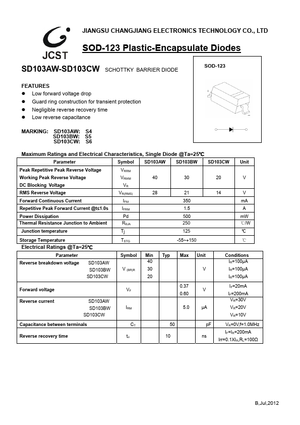
z Low forward voltage drop z Guard ring construction for transient protection z Negligible reverse recovery time z Low reverse capacitance MARKING: SD103AW: S4 SD103BW: S5 SD103CW: S6
MAXIMUM RATINGS
and
ELECTRICAL CHARACTERISTICS
, Single Diode @Ta=25℃ Parameter Symbol SD103AW SD103BW SD103CW Peak Repetitive Peak Reverse Voltage VRRM Working Peak Reverse Voltage VRWM 40 30 20 DC Blocking Voltage VR RMS Reverse Voltage VR(RMS) 28 21 14 Forward Continuous Current IFM 350 Repetitive Peak Forward Current @t≤1.0s IFRM 1.5 Power Dissipation Pd 500 Thermal Resistance Junction to Ambient RθJA 250 Junction temperature Tj 125 Unit V V mA A mW ℃/W ℃ Storage Temperature Electrical Ratings @Ta=25℃ Parameter Reverse breakdown voltage SD103AW SD103BW SD103CW TSTG Symbol V (BR)R Min 40 30 20 -55~+150 Typ Max Unit V ℃ Conditions IR=100μA IR=100μA IR=100μA Forward voltage Reverse current SD103AW SD103BW SD103CW VF IRM 0.37 0.60 5.0 V μA IF=20mA IF=200mA VR=30V VR=20V VR=10V Capacitance between...
This website uses cookies or similar technologies, to enhance your browsing experience and provide personalized recommendations. By continuing to use our website, you agree to our Privacy Policy