Datasheet Details
| Part number | JCWT8CN2ES6 |
|---|---|
| Manufacturer | JIACANWEI |
| File Size | 1.29 MB |
| Description | N-Channel Enhancement Mode Field Effect Transistor |
| Download | JCWT8CN2ES6 Download (PDF) |
|
|
|
Overview: JCWT8CN2ES6 N-Channel Enhancement Mode Field Effect Transistor Marking and pin assignment Product Summary ● VDS ● ID ● RDS(ON)( at VGS=4.5V) ● RDS(ON)( at VGS=2.5V) ● RDS(ON)( at VGS=1.
| Part number | JCWT8CN2ES6 |
|---|---|
| Manufacturer | JIACANWEI |
| File Size | 1.29 MB |
| Description | N-Channel Enhancement Mode Field Effect Transistor |
| Download | JCWT8CN2ES6 Download (PDF) |
|
|
|
● Trench Power LV MOSFET technology ● High Power and current handing capability
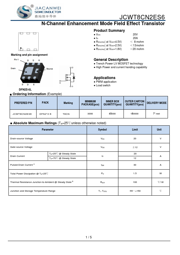
 DFN2*2-6L ■ Ordering Information (Example) PREFERED P/N PACK Marking Applications ● PWM application ● Load switch MINIMUM PACKAGE(pcs) INNER BOX QUANTITY(pcs) OUTER CARTON QUANTITY(pcs) DELIVERY MODE JCWT8CN2ES6 DFN2*2-6 T8CN 3000 45000 ■ Absolute Maximum Ratings (TA=25℃unless otherwise noted) Parameter Symbol Drain-source Voltage VDS Gate-source Voltage VGS TA=25℃ @ Steady State Drain Current TA=70℃ @ Steady State ID Pulsed Drain Current A IDM Total Power Dissipation @ TA=25℃ PD Thermal Resistance Junction-to-Ambient @ Steady State B RθJA Junction and Storage Temperature Range TJ ,TSTG 180000 7“ reel Limit 20 ±12 20 12 30 1.5 100 -55~+150 Unit V V A A W ℃/ W ℃ 1/5 ■ Electrical Characteristics (TJ=25℃ unless otherwise noted) Parameter Symbol Conditions Static Parameter Drain-Source Breakdown Voltage Zero Gate Voltage Drain Current Gate-Body Leakage Current BVDSS IDSS IGSS VGS= 0V, ID=250μA VDS=20V,VGS=0V,TC=25℃ VGS= ±10V, VDS=0V Gate Threshold Voltage VGS(th) VDS= VGS, ID=250μA VGS= 4.5V, ID=6.8A Static Drain-Source On-Resistance RDS(ON) VGS= 2.5V, ID=3.0A VGS= 1.8V, ID=2.5A Diode Forward Voltage VSD IS=6A,VGS=0V Maximum Body-Diode Continuous Current IS Dynamic Parameters Input Capacitance Ciss Output Capacitance Coss VDS=10V,VGS=0V,f=1MHZ Reverse Transfer Capacitance Crss Switching Parameters Total Gate Charge Qg Gate Source Charge Qgs VGS=4.5V,VDS=10V,ID=6A Gate Drain Charge Qgd Turn-on Delay Time tD(on) Turn-on Rise Time Turn-off Delay Time tr tD(off) VGS=4.5V,VDD=10V, RL=1.5Ω, RGEN=3Ω Turn-off Fall Time tf A.
Pulse Test: Pulse Width≤300us,Duty cycle ≤2%.
B.
Compare JCWT8CN2ES6 distributor prices and check real-time stock availability from major suppliers. Prices and inventory may vary by region and order quantity.
| Part Number | Description |
|---|