C2331 Overview
Description
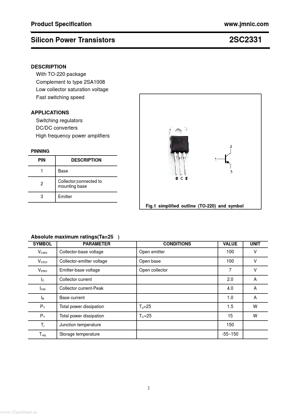
¡¤ With TO-220 package ¡¤ Complement to type 2SA1008 ¡¤ Low collector saturation voltage ¡¤ Fast switching speed APPLICATIONS ¡¤ Switching regulators ¡¤ DC/DC converters ¡¤ High frequency power amplifiers PINNING PIN 1 2 3 Base Collector;connected to mounting base Emitter Fig.1 simplified outline (TO-220) and symbol DESCRIPTION SYMBOL VCBO VCEO VEBO IC ICM IB PT PT Tj Tstg PARAMETER Collector-base voltage Collector-emitter voltage Emitter-base voltage Collector current Collector current-Peak Base current Total power dissipation Total power dissipation Junction temperature Storage temperature Ta=25¡æ TC=25¡æ CONDITIONS Open emitter Open base Open collector VALUE 100 100 7 2.0 4.0 1.0 1.5 15 150 -55~150 ¡æ ¡æ UNIT V V V A A A W W 2 Product Specification Silicon Power Transistors CHARACTERISTICS Tj=25¡æ unless otherwise specified PARAMETER Base-emitter sustaining voltage Collector-emitter saturation voltage Base-emitter saturation voltage Collector cut-off current Emitter cut-off current DC current gain DC current gain CONDITIONS IC=1.0A ,IB=0.1A,L=1mH IC=1A; IB=0.1A IC=1A ;IB=0.1A VCB=100V; IE=0 VEB=5V; IC=0 IC=0.1A ; VCE=5V IC=1A ; VCE=5V 40 40 MIN 100 TYP. SYMBOL VCEO(SUS) VCEsat VBEsat ICBO IEBO hFE-1 hFE-2 2SC2331 MAX UNIT V 0.6 1.5 10 10 ¦Ì ¦Ì V V A A 200 Switching times resistive load ton ts tf Turn-on time Storage time Fall time IC=1.0A IB1=- IB2=0.1A RL=50¦¸ ;VCC¡Ö 50V 0.5 1.5 0.5 ¦Ì ¦Ì ¦Ì s s s hFE-2 Classifications M 40-80 L 60-120 K 100-200 3 Product Specification Silicon Power Transistors PACKAGE OUTLINE 2SC2331 Fig.2 Outline dimensions(unindicated tolerance:¡À 0.10 mm) 4.