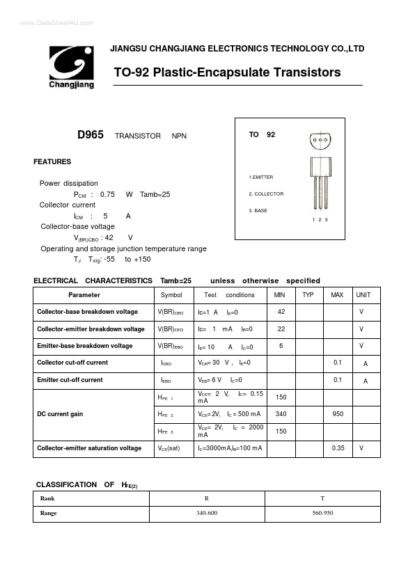
D965
FEATURES
TRANSISTOR£¨NPN £©
TO¡ª 92
1.EMITTER
Power dissipation PCM : 0.75 W£¨ Tamb=25¡æ£© Collector current ICM : 5 A Collector-base voltage V(BR)CBO : 42 V Operating and storage junction temperature range T J £¬ T stg: -55¡æto +150¡æ ELECTRICAL CHARACTERISTICS£¨ Tamb=25¡æ
Parameter Collector-base breakdown voltage Collector-emitter breakdown voltage Emitter-base breakdown voltage Collector cut-off current Emitter cut-off current Symbol V(BR)CBO V(BR)CEO V(BR)EBO ICBO IEBO HFE£¨ 1£© DC current gain HFE£¨ 2£© HFE£¨ 3£© Collector-emitter saturation voltage VCE(sat)
2. COLLECTOR
3. BASE
1 2 3 unless
Test otherwise
MIN 42 22 6 specified£©
TYP MAX UNIT V V V 0.1 0.1 ¦Ì A ¦Ì A conditions
Ic=1m A£¬IE=0 Ic= 1 IE= 10 m A£¬IB=0 ¦Ì A£¬IC=0
VCB= 30 V , IE=0 VEB= 6 V£¬IC=0 VCE= 2 V, m A VCE= 2V, VCE= 2V, m A IC= 0.15 150 340 150
IC = 500 m A IC = 2000
IC=3000m A,IB=100 m A
CLASSIFICATION OF H FE(2)
Rank Range R 340-600 T 560-950
TO-92 PACKAGE OUTLINE...