Jiangsu Changjiang Electronics K596
Si N-CHANNEL JUNCTION FET
| Part No. | K596 |
|---|---|
| Datasheet | K596 Download |
| Manufacturer |  Jiangsu Changjiang Electronics |
| Description | Si N-CHANNEL JUNCTION FET |
| Buy | Stock & Price |

FEATURES
Power dissipation PCM: 0.1W£¨ Tamb=25¡æ£© Gate Current I G: 10mA Drain current I D : 1mA Drain-Source voltage BVGDO: -20 V Operating and storage junction temperature range T J £¬ T stg: -55¡æto +150¡æELECTRICAL CHARACTERISTICS
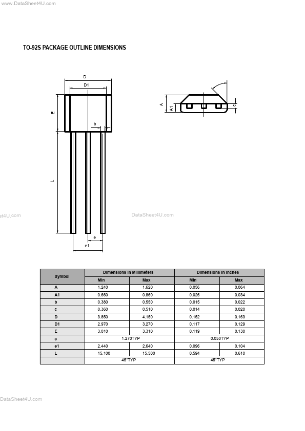
£¨ Tamb=25¡æ Parameter Gate-Drain breakdown Voltage Gate-Source cut-off Voltage Drain Current Forward Transfer Admittance Input Capacitance Symbol 2.GATE 3.DRAIN 123 unless otherwise specified£© MIN -20 -0.6 100 0.4 1.2 3.5 -1.5 800 TYP MAX UNIT V V ¦Ì A mS pF Test conditions IG= -100¦Ì A BVGDO DataSheet4U.com VGS(off) IDSS |YFS| Ciss VDS= 5V , ID=1¦Ì A VDS= 5 V , VGS=0 VDS= 5V , VGS=0, f=1KHz VDS=5V, VGS=0, f=1MHz VDS= 5 V, V GS=0 DataShee Output Capacitance CRSS 0.65 pF f = 1MHz IDSS Classification Classification IDSS (µA) A 100-170 B 150-240 C 210-350 D 320-480 E 440-800 DataSheet4U.com et4U.com DataSheet4U.com DataShee DataSheet4U.com TO-92S PACKAGE OUTLINE DIMENSIONS D D1 ¦È A E b L et4U.com DataSheet4U.com e e1 Symbol A A1 b c D D1 E e e1 L ¦È Dime...