Datasheet4U Logo Datasheet4U.com

KHB011N40F2 - N CHANNEL MOS FIELD EFFECT TRANSISTOR

General Description

This planar stripe MOSFET has better characteristics, such as fast switching time, low on resistance, low gate charge and excellent avalanche characteristics.

Key Features

  • VDSS(Min. )= 400V, ID= 10.5A Drain-Source ON Resistance : RDS(ON)=0.53 @VGS =10V Qg(typ. ) =32.5nC K M L J D N N P F G H I J 15.95 MAX 1.3+0.1/-0.05 _ 0.1 0.8 + _ 0.2 3.6 + _ 0.1 2.8 + 3.7 0.5+0.1/-0.05 1.5 _ 0.3 13.08 + 1.46 _ 0.1 1.4 + _ 0.1 1.27 + _ 0.2 2.54 + _ 0.2 4.5 + _ 0.2 2.4 + _ 0.2 9.2 + H K L M N O P Q 1 2 3.

📥 Download Datasheet

Datasheet Details

Part number KHB011N40F2
Manufacturer KEC
File Size 527.25 KB
Description N CHANNEL MOS FIELD EFFECT TRANSISTOR
Datasheet download datasheet KHB011N40F2 Datasheet

Full PDF Text Transcription (Reference)

The following content is an automatically extracted verbatim text from the original manufacturer datasheet and is provided for reference purposes only.

View original datasheet text
www.DataSheet4U.com SEMICONDUCTOR TECHNICAL DATA KHB011N40P1/F1/F2 N CHANNEL MOS FIELD EFFECT TRANSISTOR General Description 
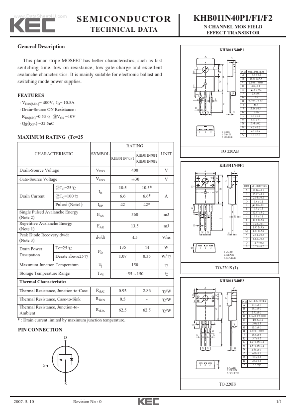
A KHB011N40P1 O C F E G B Q I DIM MILLIMETERS _ 0.2 9.9 + A B C D E This planar stripe MOSFET has better characteristics, such as fast switching time, low on resistance, low gate charge and excellent avalanche characteristics. It is mainly suitable for electronic ballast and switching mode power supplies. FEATURES VDSS(Min.)= 400V, ID= 10.5A Drain-Source ON Resistance : RDS(ON)=0.53 @VGS =10V Qg(typ.) =32.5nC K M L J D N N P F G H I J 15.95 MAX 1.3+0.1/-0.05 _ 0.1 0.8 + _ 0.2 3.6 + _ 0.1 2.8 + 3.7 0.5+0.1/-0.05 1.5 _ 0.3 13.08 + 1.46 _ 0.1 1.4 + _ 0.1 1.27 + _ 0.2 2.54 + _ 0.2 4.5 + _ 0.2 2.4 + _ 0.2 9.