KEC KIC7253T5
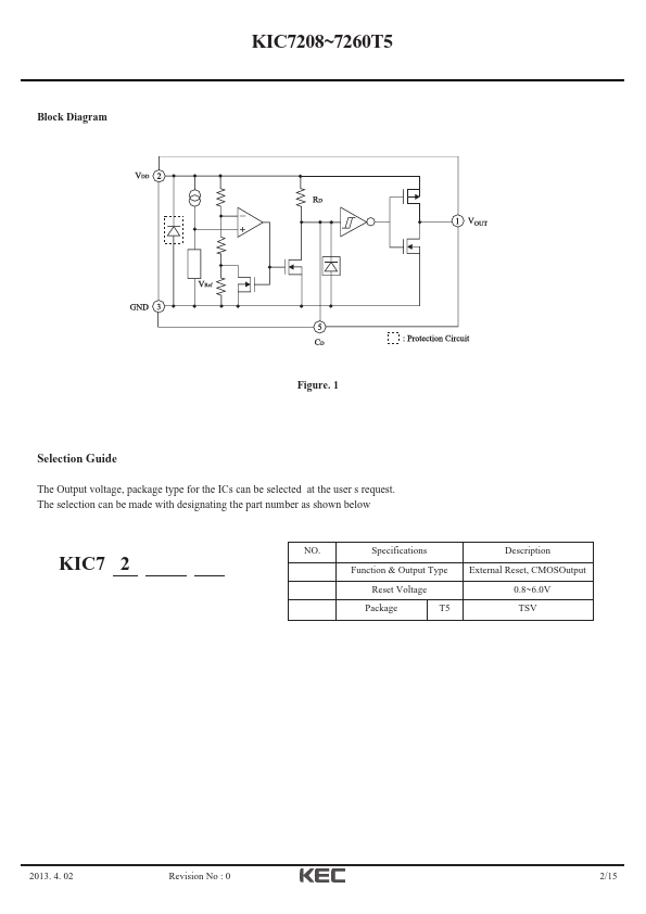
The Output voltage, package type for the ICs can be selected at the user s request. The selection can be made with designating the part number as shown below KIC7 2 NO.| Part No. | KIC7253T5 |
|---|---|
| Datasheet | KIC7253T5 Download |
| Manufacturer |  KEC |
| Description | CMOS System Reset IC |
| Buy | Stock & Price |
FEATURES
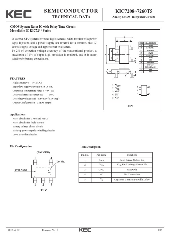
High accuracy : 1% MAX Super low supply current : 0.35 A typ. Operating-temperature range : -40~+105 Delay resistance accuracy :10 10% Detecting voltage rank : 0.8~6.0V(0.1V step) Output Configuration : CMOS outputAPPLICATIONS
Reset circuits for CPUs and MPUs Reset circuits for logic circuits Battery voltage check circuits Back-up power supply switching circuits Level detection circuits Pin Configuration PinDESCRIPTION
Pin No. 1 2 3 4 5 Pin name VOUT VDD GND NC CD Functions Reset Signal Output Pin VDD Pin / Voltage Detect Pin GND Pin No Connection Capacitor Connect Pin with Delay 2013. 4. 02 Revision No : 0 1/15 Block Diagram KIC7208~7260T5 Figure. 1 Selection Guide SpecificationsDESCRIPTION
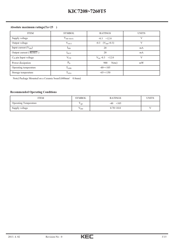
Function & Output Type External Reset, CMOSOutput Reset Voltage 0.8~6.0V Package T5 TSV 2013. 4. 02 Revision No : 0 2/15 KIC7208~7260T5 Absolute maximum ratings(Ta=25 ) ITEM SYMBOL Supply voltage Output voltage Input current (VDD) Output current ( RESET ) CD pin Input voltage Power dissipation Operating temperature Storage temperature VDD MAX.