KIC7256T5
Description
Function & Output Type External Reset, CMOSOutput Reset Voltage 0.8~6.0V Package T5 TSV 2013.
Key Features
- High accuracy : 1% MAX Super low supply current : 0.35 A typ
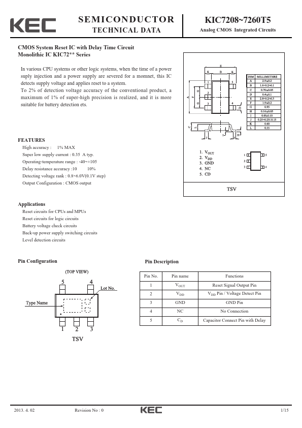
Function & Output Type External Reset, CMOSOutput Reset Voltage 0.8~6.0V Package T5 TSV 2013.