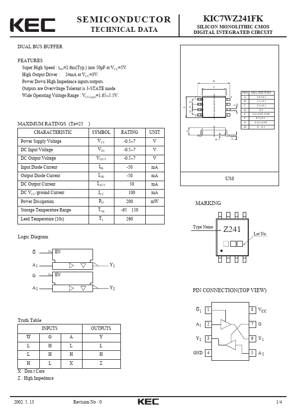
KIC7WZ241FK Key Features
- 65 150 260
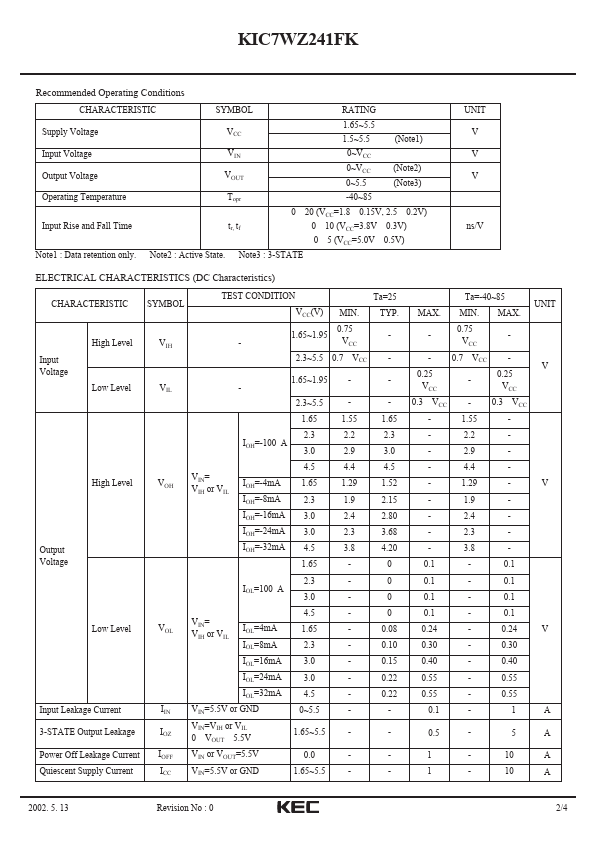
- 1.65~1.95
- 2.3~5.5
- 0.7 VCC
- 0.3 VCC
- IOH=-100 A
- High Level
- IOH=-16mA 3.0
- IOH=-24mA 3.0
- Output Voltage
| Part Number | Description |
|---|---|
| KIC7WZ240FK | DUAL BUS BUFFER |
| KIC7WZ00FK | 2-INPUT NAND GATE |
| KIC7WZ02FK | 2-INPUT NOR GATE |
| KIC7WZ04FK | TRIPLE INVERTER |
| KIC7WZ05FK | TRIPLE INVERTER |